
Summaries of my Professional Projects
Click any of the project titles below to read about them.
Each description gives a high level “inside story”, talking about the motivations, strategic vision, technical challenges, and outcomes.
For the deeper technical details of each project, take a look at the Related Publications that are listed at the end of each project description.
Projects at imec
Leuven, Belgium
2013 – 2021
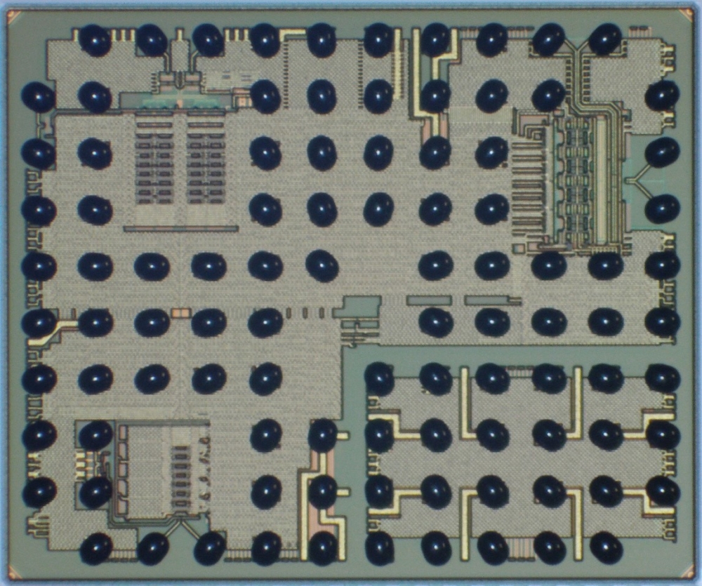
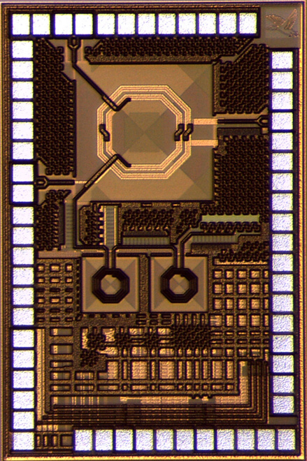
2020 --- Ringamp-Based Pipelined-SAR with Comprehensive Background Calibration
Ringamp-Based Pipelined-SAR with Full Background Calibration and Record Breaking Efficiency
Technology: 16nm FinFET CMOS
Time Period: October 2019 – December 2020
Collaborators: Nereo Markulic, Jorge Lagos, Jan Craninckx
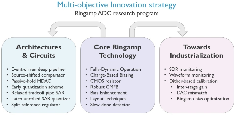 My general philosophy and approach to integrated circuit design research is to pursue innovation on multiple levels, in parallel. Circuits and systems tend to be particularly compatible to this approach because core block-level ideas can often be compartmentalized inside of broader system-level ideas. In the case of the 16nm ringamp ADC program that I ran at imec, this consisted of three parallel tracks spanning several design generations: block-level ringamp innovation, system-level architectures and circuits, and industrialization techniques.
The high speed ringamp topology that we developed and used in the previous design iteration was the culmination of many years of work and refinement. It is an elegant, nuanced, and effective topology for high speed, high efficiency residue amplification. We were quite content to continue to use it in this design iteration, and instead focus fully on making important statements on the architectural and industrialization side of things.
With regard to architecture, one critique that can be made of the previous “deep” pipeline architectures used in the previous imec ringamp ADCs is that they are not as power and efficiency optimized as they could be when compared with other architectures. This was a conscious choice that we made, and our 1.5b/stage deep pipeline architectures have their own compelling set of benefits. But it did lead to the false impression among some people that for very efficiency-critical applications ringamps might not be as good as Gm-C and Gm-R amplifiers. We wanted to set the record straight on this, and set out to build a 500MS/s ringamp-based pipelined-SAR ADC (5x the speed of all previous ringamp-based pipelined SARs) and the best power efficiency of any single-channel ADC above 200MS/s. In other words, we wanted to switch architectures from pipeline to pipelined-SAR in order to show how ringamps are a versatile block-level solution that can redefine design tradeoffs of any architecture, and enable advances in state-of-the-art performance across-the-board. This broad versatility is, fundamentally, what sets ringamps apart from other modern scalable amplifier ideas out there, so it is important to demonstrate this key point to the broader circuits community. We also continued at the architecture level to refine our previous ideas on reference voltage regulation, both improving the fully-dynamic “split-reference” regulation technique at circuit level and also showing how it can be used within a pipelined-SAR context.
 On the industrialization side of things, we took a different and somewhat more traditional approach to background monitoring and optimization of the ringamp this time around. In the previous two designs we had tinkered with “sensing” based methods of calibration enabled by stochastic ADC monitor circuits: SDR estimation, and transient waveform capture. In this design, we switched gears and looked into dither-based calibration methods. What we found excited us. Dither-based methods appear to be very promising as a ringamp industrialization technique, not only because they are robust and can be easily modeled in system-level verification, but also because they can be reused for calibrating many other types of errors. For example, in this design we use a single, simple dither system to calibrate all important sources of error in our system, including ringamp biasing optimality, interstage gain, and capacitor DAC mismatch.
Overall, we crammed a lot of ideas into this project, in accordance with a philosophy of innovating across all levels of the design. Amongst all of these ideas, I am the most satisfied with the dither-based optimization of ringamp performance. It is simple, elegant, and based on a concept that is already widely used and will thus be easily understood and readily accepted by others in the field. With this project, and the three different industrialization solutions for ringamps we developed over the 3-phase roadmap of the 16nm ringamp ADC program at imec, I feel confident that ringamps can be used in actual commercial products. Other researchers have shown how ringamps can be made PVT robust using analog design techniques and design margin, and we showed in the imec research program how they can also be made PVT robust by using digital calibration techniques. There are now many options available to designers.
Our measurement campaign went well, and, like the previous designs, we exploited the philosophy of using the chip as a “real world simulator” to get the most knowledge, insight, and learning out of our testing time in the lab. A paper summarizing the design was accepted to VLSI 2021. We plan to expand with a longer journal paper in the future.
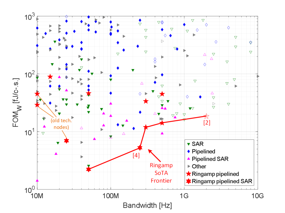 This particular project marks for me an important milestone. It is the culmination of a decade long journey that I began when I simulated the first ringamp circuit during my PhD years. Ever since, I have viewed ringamps as a paradigm with great potential to solve a long standing and fundamental challenge in switched capacitor circuits. I never let go of that vision, and continued to push for an answer to the questions: “will it ever actually work?” and “can it help to advance the frontiers of technology?”. I now feel that I’ve found a satisfactory answer to both of these questions. Ringamps are not only at a point of maturity that they are ready to be used in commercial applications, but there are already some companies with ringamps in existing products. They are a fundamental block level solution that is helping to redefine the landscape of real-world system level challenges and is helping to push the boundaries and capabilities of technology. If you look at the famous Murmann ADC Survey plots, you will see that ringamp-based ADC designs now form a line across the leading edge of the FoM performance boundary, from 100MS/s up to 4GS/s. Slowly but surely, the data is coming in, and it is telling us that ringamps are perhaps the most general solution we have found yet for a truly technology-scalable switched-capacitor amplifier. Meanwhile, I now have the satisfaction and excitement of seeing at almost every circuits conference in the last few years new designs using ringamps, and new ideas and perspectives being proposed. Ringamp-based LDOs, ringamp-based delta-sigmas, ringamp-based PLLs, self-quenching ringamps, and more. For a long time, it has felt to me like this crazy ringamp idea would not survive and grow without my dedication and commitment to keep carrying the torch. There have been some other very important contributors to the topic over the years, but no torch bearers. I think that era of carrying the torch alone is finally over, and other people are joining and bringing fresh ideas and insights to the topic. I’m very excited to see where other people in the circuits community can take ringamps next!
Related Publications:
A 10.0 ENOB, 6.2 fJ/conv.-step, 500 MS/s Ringamp-Based Pipelined-SAR ADC with Background Calibration and Dynamic Reference Regulation in 16nm CMOS
J. Lagos, N. Markulic, B. Hershberg, D. Dermit, M. Shrivas, E. Martens, and J. Craninckx
In 2021 Symposium on VLSI Circuits, June, 2021.
» [Paper] [DOI] [Abstract] [Bibtex]
@INPROCEEDINGS{2021-vlsi-type3,

author={Lagos, J. and Markulic, N. and Hershberg, B. and Dermit, D. and Shrivas, M. and Martens, E. and Craninckx, J.},

booktitle={{2021 Symposium on VLSI Circuits}},

title={{A 10.0 ENOB, 6.2 fJ/conv.-step, 500 MS/s Ringamp-Based Pipelined-SAR ADC with Background Calibration and Dynamic Reference Regulation in 16nm CMOS}},

year={2021},

volume={},

number={},

pages={1-2},

abstract={We present a single-channel fully-dynamic pipelined SAR ADC that leverages a novel quantizer and narrowband dither injection to achieve fast and comprehensive background calibration of DAC mismatch, interstage gain, and ring amplifier (ringamp) bias optimality. The ADC also includes an on-chip wide-range, fully-dynamic reference regulation system. Consuming 3.3 mW at 500 MS/s, it achieves 10.0 ENOB and 75.5 dB SFDR, yielding a Walden FoM of 6.2 fJ/c.s.},

keywords={},

doi={10.23919/VLSICircuits52068.2021.9492354},

ISSN={2158-5636},

month={June},

type={conference}}
…and a journal paper expansion to be posted here when it becomes available.
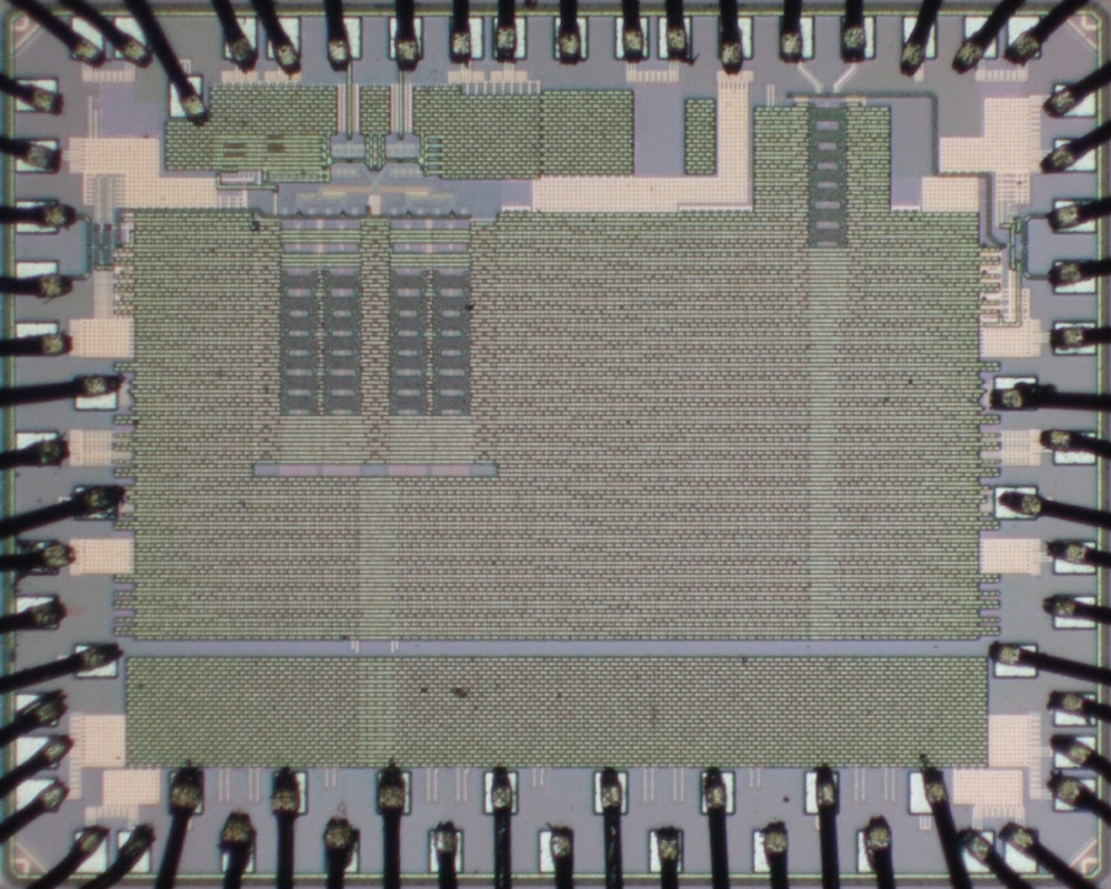
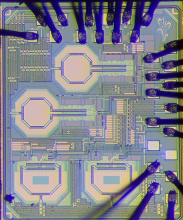
2019 --- Dynamic Reference Regulation and Scope-on-Chip
Fully-Dynamic Reference Regulation and Scope-on-Chip Transient Waveform Capture
Technology: 16nm FinFET CMOS
Time Period: October 2018 – December 2019
Collaborators: Nereo Markulic, Jorge Lagos, Jan Craninckx
 The previous project, focused on a 4GS/s direct-RF ADC, succeeded in demonstrating that record breaking reconfigurable high speed ringamp-based ADCs in nanoscale CMOS are possible. Included in that architecture was an idea for signal-to-distortion (SDR) monitoring that would allow for background monitoring and optimization of ringamp settling behavior for the purposes of developing robust solutions for ringamp industrialization into commercial products. Until that point, all other researchers dabbling in ringamps tended to focus on calibration-free robustness methods, and so I felt that our efforts at imec would be best spent by investigating a different approach. Namely: lightweight calibration-based solutions. This can in theory allow for higher speeds of operation than purely analog-based robustness methods. The SDR monitor of the earlier project was an important first step in this industrialization research roadmap, and showed one possible solution. However, most difficult problems usually require experimenting with multiple approaches. Sometimes a clear winner emerges. Other times, each comes with pros and cons, and each fits better into certain application contexts than others. And sometimes, the idea grows into something else entirely, and leads in unexpected directions. In the invention process, you don’t always need to know exactly where you’re going when you set out. In fact, sometimes its better that you don’t.
This project focused on the general theme of industrialization of ringamp-based pipelined ADCs, with two primary innovations. The first was a new solution for ringamp background monitoring and optimization based on stochastic transient waveform capture, which added another approach to ringamp PVT robustness in addition to the SDR technique of the previous project. The second key focus was on the supporting systems outside of the core ADC. The architecture is fully-dynamic and event-driven, and as such, it is capable of a constant energy-per-conversion, making it fully speed reconfigurable. That is, it is energy efficient regardless of what speed you clock it at. Outside of the core ADC, there is still supporting circuitry required, and not all of this is guaranteed to also be fully-dynamic. In particular, the voltage regulators for the supply and precision reference lines. To address this, in this design we developed a new type of voltage regulation system that is also fully dynamic, thereby extending our speed reconfigurability advantage to the system level.
In the lab, we saw great results and learned a lot. I am a strong proponent of using the universe as a simulator. That is, rather than trying to perfectly model and simulate everything in advance and tape out a fairly inflexible design, I prefer to build in many digitally controllable ideas, options, and test modes. For research, where there is room for a bit of prototyping, this makes time in the lab much more valuable. Rather than only using measurement to validate, this approach turns measurement into a key part of the research process, where hypotheses can be explored with actual silicon and real electrons. In this regard, we learned quite a bit from this chip. The regulator system had many operating modes, and we learned very quickly about what works, what is robust, and what isn’t. Likewise, the scope-on-chip transient waveform capture idea was very well suited for in-situ investigation because it is stochastic in nature and requires both a large number of samples and real-world noise processes to operate. This would be very tedious to simulate in a CAD tool, but in real silicon, we were able to learn and refine our understanding very rapidly. The highlight of this project for me was seeing actual transient waveform captures of ringamp settling behavior, obtained by the scope-on-chip circuit. I was the first time I (or anyone) had actually seen this data. I simulate and analyze ringamp waveforms all the time in the CAD environment – but to see proof that this really is what is happening inside the chip at atomic scale is just very exciting! Although we used the waveform capture system to demonstrate a solution for ringamp industrialization, I do have some concerns that it is too dependent on heuristics to be fully reliable. It is the solution that we came up with next, in the subsequent project, that I have the most faith in. But either way, I consider this project, and the scope-on-chip system a great success because it showed a way to probe internal nets of an ADC in real silicon in a very non-invasive way. For test and debug diagnostics, and applications outside of ringamps entirely, this is interesting and new. This is an example of an idea that could eventually evolve beyond the application it was originally intended for. We’ll see!
This architecture was an upgrade of the “mobile” version of the previous project, with a target to hit 1MS/s – 1GS/s fully dynamic operation and 9.5 ENOB. We met all of these goals. The results were first disclosed at VLSI 2020, and later appeared as an invited journal paper in JSSC.
Related Publications:
A 1MS/s to 1GS/s Ringamp-Based Pipelined ADC with Fully Dynamic Reference Regulation and Stochastic Scope-on-Chip Background Monitoring in 16nm
B. Hershberg, N. Markulic, J. Lagos, E. Martens, and J. Craninckx
In 2020 Symposium on VLSI Circuits, June, 2020.
» [Paper] [Video] [DOI] [Abstract] [Bibtex]
@INPROCEEDINGS{2020-vlsi-type2-4d,

author={B. {Hershberg} and N. {Markulic} and J. {Lagos} and E. {Martens} and J. {Craninckx}},

booktitle={{2020 Symposium on VLSI Circuits}},

title={{A 1MS/s to 1GS/s Ringamp-Based Pipelined ADC with Fully Dynamic Reference Regulation and Stochastic Scope-on-Chip Background Monitoring in 16nm}},

year={2020},

volume={},

number={},

pages={1-2},

abstract={This paper presents an 11 bit fully dynamic pipelined ADC with an integrated reference buffer that consumes only 8% of total power. It operates from 1MS/s to 1GS/s and maintains 59.5dB SNDR and 14fJ/conv-step FoMW across this range. Furthermore, a small circuit is introduced that provides background reconstruction of amplifier settling behavior.},

keywords={analogue-digital conversion;operational amplifiers;reference circuits;stochastic processes;fully dynamic reference regulation;stochastic scope-on-chip background monitoring;pipelined ADC;integrated reference buffer;ring amp-based pipelined ADC;amplifier background reconstruction;Monitoring;Regulators;Clocks;Power demand;Capacitors;Pipelines;Detectors},

doi={10.1109/VLSICircuits18222.2020.9162788},

ISSN={2158-5636},

month={June},

video={https://youtu.be/MXVd0AmaYz0},

type={conference}}
A 1-MS/s to 1-GS/s Ringamp-Based Pipelined ADC With Fully Dynamic Reference Regulation and Stochastic Scope-on-Chip Background Monitoring in 16 nm
B. Hershberg, N. Markulić, J. Lagos, E. Martens, D. Dermit, and J. Craninckx
In IEEE Journal of Solid-State Circuits, April, 2021.
» [Paper] [DOI] [Abstract] [Bibtex]
@ARTICLE{2021-jssc-type2-4d,

author={Hershberg, Benjamin and Markulić, Nereo and Lagos, Jorge and Martens, Ewout and Dermit, Davide and Craninckx, Jan},

journal={{IEEE Journal of Solid-State Circuits}},

title={{A 1-MS/s to 1-GS/s Ringamp-Based Pipelined ADC With Fully Dynamic Reference Regulation and Stochastic Scope-on-Chip Background Monitoring in 16 nm}},

year={2021},

volume={56},

number={4},

pages={1227-1240},

abstract={This article presents a fully dynamic ringamp-based pipelined ADC with integrated reference buffer that operates from 1-MS/s to 1-GS/s and maintains a Walden Figure-of-Merit (FoM) of 14 fJ/conversion-step across this range. A “split-reference” regulation technique is introduced, which provides multiple buffered replicas with varying accuracies and output impedances to the core ADC circuitry, relaxing overall buffer design requirements and improving efficiency. The regulator blocks are implemented with fully dynamic discrete-time loops. Furthermore, a technique for background reconstruction of residue amplifier settling behavior is also described. The “scope-on-chip” captures high-resolution transient waveforms using a 1-bit stochastic ADC. It is shown how these waveform data can be used for optimization of ringamp biasing and PVT tracking. The ADC is fabricated in a 16-nm CMOS technology and at 1 GS/s with a Nyquist input achieves 59.5-dB SNDR, 75.9-dB SFDR, and 10.9-mW total power consumption with only 8% consumed by the reference regulation.},

keywords={},

doi={10.1109/JSSC.2020.3044831},

ISSN={1558-173X},

month={April},

type={journal}}
2017 --- Direct-RF Sampling Ringamp ADC in 16nm
Asynchronous Event-Driven Direct-RF Sampling Ringamp ADCs
Technology: 16nm FinFET CMOS
Time Period: April 2016 – present
Collaborators: Barend van Liempd, Davide Dermit, Nereo Markulic, Jorge Lagos, Ewout Martens, Jan Craninckx
 By 2016 I had built up enough internal support at imec to pursue my vision to launch a full main-track research program focusing on ringamp-based ADCs. Innovation is as much about communication and securing buy-in from key players in the community (be it academic, corporate, society, or otherwise) as it is about technical merit and hard facts. I found this to be true both inside my work environment and outside in the broader circuit design community. I knew that the work I had done in my PhD was not enough to convince many skeptics, especially because it was done in a relatively old 0.18um CMOS technology which made it difficult to evaluate the true potential of ringamps. I was personally very excited about the topic, because I understood its potential, but I also did not at that point know enough yet to say whether ringamps could actually be industrialized for real commercial products. It was something that I felt deserved more study and innovation.
In the time between my PhD and the start of the ringamp roadmap at imec, a few other researchers around the world had picked up the ringamp topic too and started publishing designs with record breaking power efficiency numbers – a very good sign to be sure. However, most of the designs being published targeted lower speeds, and this began to create the misconception that ringamps were themselves limited to lower speeds. It thus felt important to correct this misconception by demonstrating high speed ringamp designs. Our 28nm designs already managed to achieve high speeds, up to 1GS/s per channel, but due to certain technology limitations and design choices, they only achieved good but not incredible power efficiencies and linearities. The goal and needs of this ADC project in 16nm CMOS in the context of the larger ringamp research roadmap was thus clear: to go where no one had gone before, and prove that ringamps could enable circuits and systems with state of the art linearity and speed and power efficiency all at once. Based on internal strategic considerations, we set out on a roadmap to build a 4GS/s ADC for use in high performance direct-RF sampling systems, a spec and application target that was well aligned with imec partner interests.
 The project initially started out with a fairly manageable scope on a reasonable timeline, with modest technical and innovation goals. But as I began developing the architecture, I saw many opportunities for new techniques and tricks and my enthusiasm to make a strong statement with this design ultimately expanded the project into what can only be described as an “absolute beast”. It included innovations in the pipelined ADC MDAC, adopted a modular event-driven asynchronous clocking approach, provided a unique solution for background monitoring and optimizing ringamp performance using a somewhat magical stochastic quantization method, and of course included a new-and-improved ringamp topology that built on our learnings from the prior 28nm ringamp pipelined ADCs. Not only did the architecture become novel and complex, but I also expanded the physical deliverables to two complementary stand-alone ADCs – one seeking the original 4GS/s 13-bit target for direct-RF base-station applications, and the other seeking a 1GS/s 11-bit target for mobile device applications. The reason to expand into two ADCs was twofold. First, it allowed us to demonstrate the unique reconfigurability advantages of the architecture: by combining a modular low-bits-per-stage pipeline with a decentralized event-driven clocking paradigm, the ADC can rapidly be reconfigured for any speed and any resolution, without performance penalty. The “mobile” version of the architecture was simply a spin-off of the larger base-station version, and benefitted very heavily from modularity and design re-use. Second, there were so many new ideas in the architecture, I knew we couldn’t possibly fit them all into a single ISSCC paper. I view ISSCC as a very important venue that can provide unparalleled exposure to promote ideas and gain traction and buy-in from the community. Every bright-eyed PhD student sitting in that audience is a potential recruit. Every professor with an open mind is a potential ally. Anyway, I knew that to fully present this design, we would need to spread it out across two papers, and that would be most likely to succeed if we had two “separate” ADCs to publish.
Scope creep of this magnitude means a lot of work and a heck of a lot of overtime, but it was both justified and necessary in this case in order to achieve the primary research objectives. (And by a lot of overtime, I mean a LOT of overtime!). Ultimately, the chip taped out, and when we got it into the lab, I saw in measurements that our efforts had paid off. Despite a few non-fatal bugs, the ADCs worked, and the overall performance made a strong statement – that ringamps are a general purpose tool for switched capacitor signal processing that can achieve both high speed and high linearity all while maintaining state of the art power efficiency. Taken all together, the total performance improvement of the direct-RF version of the ADC was roughly an order-of-magnitude better than previous state-of-the-art designs. After some bug fixes and fine-tuning on a re-tape that went out with the subsequent project, we managed to hit all of our speed targets (4GS/s for the direct-RF ADC and 1MS/s to 1GS/s for the reconfigurable mobile ADC), and came very close to our insanely ambitious 80dB linearity target, limited only by the external packaging and matching networks.
My intention to catch people’s attention at ISSCC turned out even better than I had hoped. Not only did we have the rare fortune of getting two papers accepted into a single session at ISSCC 2019, these papers were so well received that we were also awarded the Lewis Winner Award for Outstanding Paper, which is essentially the ISSCC “best paper” award. I never once in my life even considered the possibility of a best paper award at ISSCC, so this was a huge surprise. This juncture also felt, to me, like an important milestone for ringamp related research. Whereas before I had worried that without a dedicated champion/promoter like myself to keep the topic alive and on-track, by 2019 and 2020 it had started to feel like the idea could finally stand on its own. People saw the clear advantages that had been proven in silicon, they were paying attention, and new people, perspectives, enthusiasm, and topologies would soon infuse the topic with fresh energy.
It was encouraging progress to be sure, but my vision and roadmap was still incomplete. There remained the looming question of industrialization. The SDR monitoring idea in this design offered a solution in this regard, but I still felt like there was more work to be done…
Related Publications:
A 3.2GS/s 10 ENOB 61mW Ringamp ADC in 16nm with Background Monitoring of Distortion
B. Hershberg, D. Dermit, B. v. Liempd, E. Martens, N. Markulic, J. Lagos, and J. Craninckx
In 2019 IEEE International Solid- State Circuits Conference – (ISSCC), Feb, 2019.
» [Paper] [Slides] [DOI] [Abstract] [Bibtex]
@INPROCEEDINGS{2019-isscc-type1,

author={B. {Hershberg} and D. {Dermit} and B. v. {Liempd} and E. {Martens} and N. {Markulic} and J. {Lagos} and J. {Craninckx}},

booktitle={{2019 IEEE International Solid- State Circuits Conference - (ISSCC)}},

title={{A 3.2GS/s 10 ENOB 61mW Ringamp ADC in 16nm with Background Monitoring of Distortion}},

year={2019},

volume={},

number={},

pages={58-60},

abstract={This paper presents a 13b, 3.2Gsps, 4x interleaved ringamp-based pipelined ADC with Walden and Schreier FoMs of 19.2fJ/c-step and 165.9dB respectively. It introduces a general method for background tracking of signal-to-distortion ratio using a single-comparator stochastic ADC, which can be used to maintain optimal biasing of the digitally controlled fully-differential ringamp circuit. Mismatch between the SHA-less MDAC and sub-ADC is eliminated by quantizing directly from the MDAC capacitors.},

keywords={Estimation;Monitoring;Distortion;Pipelines;Capacitors;Bandwidth;Hardware},

doi={10.1109/ISSCC.2019.8662290},

ISSN={2376-8606},

month={Feb},

type={conference}}
A 6-to-600MS/s Fully Dynamic Ringamp Pipelined ADC with Asynchronous Event-Driven Clocking in 16nm
B. Hershberg, B. v. Liempd, N. Markulic, J. Lagos, E. Martens, D. Dermit, and J. Craninckx
In 2019 IEEE International Solid- State Circuits Conference – (ISSCC), Feb, 2019.
» [Paper] [Slides] [DOI] [Abstract] [Bibtex]
@INPROCEEDINGS{2019-isscc-type2,

author={B. {Hershberg} and B. v. {Liempd} and N. {Markulic} and J. {Lagos} and E. {Martens} and D. {Dermit} and J. {Craninckx}},

booktitle={{2019 IEEE International Solid- State Circuits Conference - (ISSCC)}},

title={{A 6-to-600MS/s Fully Dynamic Ringamp Pipelined ADC with Asynchronous Event-Driven Clocking in 16nm}},

year={2019},

volume={},

number={},

pages={68-70},

abstract={In this paper it is shown how an asynchronous, event-driven approach to timing control in many-stage “deep” pipelined ADCs leads to numerous advantages in efficiency, robustness, and reconfigurability. This is combined with the efficiency of ring amplifiers to build a single-channel 11b, 60dB SNDR, 78dB SFDR pipelined ADC with fully dynamic power consumption that maintains better than 13 fJ/c-step Walden FoM from 6Msps to 600Msps.},

keywords={Clocks;Timing;Pipelines;Quantization (signal);System recovery;Jitter;Protocols},

doi={10.1109/ISSCC.2019.8662319},

ISSN={2376-8606},

month={Feb},

type={conference}}
A 4-GS/s 10-ENOB 75-mW Ringamp ADC in 16-nm CMOS With Background Monitoring of Distortion
B. Hershberg, D. Dermit, B. van Liempd, E. Martens, N. Markulić, J. Lagos, and J. Craninckx
In IEEE Journal of Solid-State Circuits, Aug, 2021.
» [Paper] [DOI] [Abstract] [Bibtex]
@ARTICLE{2021-jssc-type1-direct-rf-ringamp,

author={Hershberg, Benjamin and Dermit, Davide and van Liempd, Barend and Martens, Ewout and Markulić, Nereo and Lagos, Jorge and Craninckx, Jan},

journal={{IEEE Journal of Solid-State Circuits}},

title={{A 4-GS/s 10-ENOB 75-mW Ringamp ADC in 16-nm CMOS With Background Monitoring of Distortion}},

year={2021},

volume={56},

number={8},

pages={2360-2374},

abstract={A 4x interleaved pipelined ADC for direct-RF sampling applications is presented. It leverages the performance advantages of ring amplifiers to unlock greater architectural freedom. The first pipeline stage MDAC with a “passive-hold” mode eliminates the sub-ADC sampling path and associated problems. A high-speed ringamp topology employs digital bias control, robust common-mode feedback (CMFB), and an elegant self-resetting behavior. An asynchronous, event-driven timing control system improves several aspects of performance and enables fully dynamic power consumption and modular design re-use. A general technique is presented whereby the signal-to-distortion ratio (SDR) of any amplifier in the system can be measured in the background with an analog hardware overhead of only one comparator. In this amplifier-intensive architecture utilizing 36 ringamps, the 4-GS/s ADC fabricated in 16-nm CMOS achieves 62-dB SNDR and 75-dB SFDR at Nyquist, consumes 75 mW (including input buffer), and has a Walden figure of merit (FoM) of 18 fJ/conversion-step and a Schreier FoM of 166 dB, advancing the state of the art in direct-RF sampling ADCs by roughly an order of magnitude.},

keywords={},

doi={10.1109/JSSC.2021.3053893},

ISSN={1558-173X},

month={Aug},

type={journal}}
Asynchronous Event-Driven Clocking and Control in Pipelined ADCs
B. Hershberg, B. van Liempd, N. Markulić, J. Lagos, E. Martens, D. Dermit, and J. Craninckx
In IEEE Transactions on Circuits and Systems I: Regular Papers, July, 2021.
» [Paper] [DOI] [Abstract] [Bibtex]
@ARTICLE{2021-tcas1-asynch-event-driven-clocking,

author={Hershberg, Benjamin and van Liempd, Barend and Markulić, Nereo and Lagos, Jorge and Martens, Ewout and Dermit, Davide and Craninckx, Jan},

journal={{IEEE Transactions on Circuits and Systems I: Regular Papers}},

title={{Asynchronous Event-Driven Clocking and Control in Pipelined ADCs}},

year={2021},

volume={68},

number={7},

pages={2813-2826},

abstract={An asynchronous event-driven approach to clocking and timing control is explored in the context of pipelined ADCs. It is shown how a conventional global clock tree can be replaced by localized control units coordinated through inter-stage communication protocols. The approach is found to yield many compelling advantages in terms of power efficiency, speed, robustness, and reconfigurability. It is shown how these benefits are particularly well leveraged when used in combination with dynamic-power residue amplifiers such as ring amplifiers. Several challenges also arise: re-synchronization of the digital outputs, mitigation of possible deadlock scenarios, and robust timing control configuration. Solutions to these problems are presented. Two single-channel 11-bit 1.5-bit/stage pipelined ADC designs are fabricated in a 16nm CMOS technology, each with a different implementation approach to the asynchronous control units. The trade-offs of both approaches are considered. At 1 GS/s the fastest prototype achieves 59.5 dB SNDR and 75.9 dB SFDR at Nyquist, consuming 10.9 mW including reference regulator. Due to fully-dynamic operation, it maintains a near-constant Walden Figure of Merit (FoM) of 14 fJ/conversion-step from 1 MS/s to 1 GS/s.},

keywords={},

doi={10.1109/TCSI.2021.3077881},

ISSN={1558-0806},

month={July},

type={journal}}
2016 --- Pipelined SAR ADC for High Performance Mobile
Pipelined SAR ADC for High Performance Mobile
Technology: 16nm FinFET CMOS
Time Period: 9 months (Aug 2015 – April 2016)
Collaborators: Ewout Martens, Jan Craninckx
 When I joined imec, my expectation was that I would continue my PhD work in analog mixed-signal IC design topics. Instead, I worked on RF projects for my first 3 years. That turned out to be a great opportunity, and it gave me a lot of exposure to the world of high frequency. However, all things said, mixed-signal design is still “where the party’s at” in my opinion! The added dimensional variable of “time” in sampled, mixed-signal systems opens up a lot of room for creativity. RF feels a lot closer to a classical engineering topic, with a well defined set of physical constraints. Much of the success comes down to careful modelling and optimization of circuits containing only a handful of transistors. By contrast, mixed-signal, and ADCs in particular, are a lot like coding up an algorithm, where the code is executed by electrons rather than a CPU. I’ve always been a Computer Scientist at heart, so it’s not surprising why mixed-signal appeals to me more.
Anyway, in 2015 I moved back to ADCs full-time. My first project was a continuation of imec’s highly successful SAR ADC research program. The objective was to: 1) migrate into 16nm technology 2) make a high speed 2x interleaved 14b Pipelined SAR ADC with very small area and ultra-low power. To reduce the active area, we used a new reference stabilization scheme which removed the need for decoupling capacitors or reference buffers. This was the first 16nm ADC designed at imec, so we began by studying how the 3D transistors and metal double-patterning introduced in 16nm impact design tradeoffs, modeling, and layout procedures.
My role in the project was to design the dynamic Gm-C inter-stage residue amplifier and the second stage SAR ADC. Thanks in part to the fantastic analog properties of FinFET transistors, and also with some circuit innovations, I was able to design a more efficient and more robust dynamic amplifier than the earlier designs in 28nm and 40nm planar CMOS. The second stage SAR design was my first SAR ADC project. In my PhD I had focused on pipelined ADCs. This was a fantastic learning opportunity, since the techniques and knowledge of SAR design residing at imec are world-class.
In the lab, we discovered a few design issues. Luckily, we were able to overcome these problems thanks to clever workarounds and a trip to a facility with a Focused Ion Beam (FIB). In the end, we achieved our targets and demonstrated state of the art power efficiency and area.
Related Publications:
A 16nm 69dB SNDR 300MSps ADC with capacitive reference stabilization
E. Martens, B. Hershberg, and J. Craninckx
In 2017 Symposium on VLSI Circuits, June, 2017.
» [Paper] [DOI] [Abstract] [Bibtex]
@INPROCEEDINGS{2017-vlsi-capacitive-reference-stabilization,

author={E. Martens and B. Hershberg and J. Craninckx},

booktitle={{2017 Symposium on VLSI Circuits}},

title={{A 16nm 69dB SNDR 300MSps ADC with capacitive reference stabilization}},

year={2017},

pages={C92-C93},

abstract={We present a 300 MSps 2 times interleaved pipelined SAR ADC in 16nm digital CMOS. It implements a new scheme to cancel reference voltage ripple due to DAC switching, greatly reducing requirements for decoupling capacitance and/or reference buffering, and achieves better than 76dB harmonic distortion. At 300 MSps, the peak ENOB is 11.2 bit with a power consumption of 3.6mW.},

keywords={Calibration;Clocks;Gain;Harmonic analysis;Linearity;Switches;Table lookup},

doi={10.23919/VLSIC.2017.8008559},

month={June},

type={conference}}
A 69-dB SNDR 300-MS/s Two-Time Interleaved Pipelined SAR ADC in 16-nm CMOS FinFET With Capacitive Reference Stabilization
E. Martens, B. Hershberg, and J. Craninckx
In IEEE Journal of Solid-State Circuits, April, 2018.
» [Paper] [DOI] [Abstract] [Bibtex]
@ARTICLE{2018-jssc-capacitive-reference-stabilization,

author={E. Martens and B. Hershberg and J. Craninckx},

journal={{IEEE Journal of Solid-State Circuits}},

title={{A 69-dB SNDR 300-MS/s Two-Time Interleaved Pipelined SAR ADC in 16-nm CMOS FinFET With Capacitive Reference Stabilization}},

year={2018},

volume={53},

number={4},

pages={1161-1171},

abstract={A two-time interleaved pipelined SAR ADC in 16-nm CMOS achieving 11.2-bit ENOB at 300 MS/s is presented. To cancel the signal-dependent voltage ripple on the reference node due to DAC switching, it employs a stabilization scheme based on the use of auxiliary DACs. The charge drawn from the reference becomes signal-independent, greatly reducing the requirements for the reference decoupling capacitance and/or buffers. The technique improves the linearity to levels better than 76-dB harmonic distortion. Power consumption is only 3.6 mW resulting in peak FoMs of 175.5 dB and 5.1 fJ/conv.step.},

keywords={CMOS digital integrated circuits;analogue-digital conversion;circuit stability;digital-analogue conversion;harmonic distortion;CMOS FinFET;DAC switching;auxiliary DACs;capacitive reference stabilization;harmonic distortion;power 3.6 mW;reference decoupling capacitance;reference node;signal-dependent voltage ripple cancellation;size 16 nm;stabilization scheme;two-time interleaved pipelined SAR ADC;word length 11.2 bit;Calibration;Capacitance;Capacitors;FinFETs;Harmonic distortion;Reservoirs;Switches;ADC;FinFET technology;pipelined SAR ADC;reference pre-charging;reference ripple;reference stabilization},

doi={10.1109/JSSC.2017.2784762},

ISSN={0018-9200},

month={April},

type={journal}}
2015 --- Dual-Frequency Balance Network for FDD EBDs
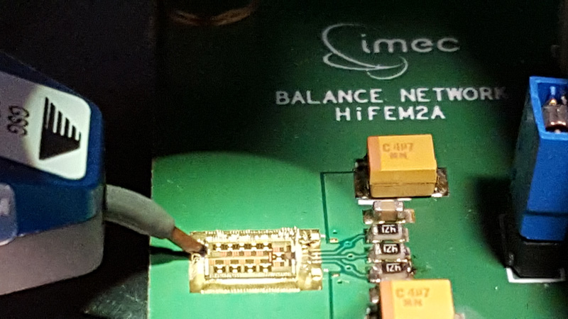
Dual-Frequency Balance Network for FDD EBDs
Technology: 180nm RF SOI CMOS
Time Period: 1.5 years (April 2014 – Aug 2015)
Collaborators: Barend van Liempd, Jan Craninckx
 Following the encouraging results of HiFEM1 (see next tab), I donned the heavy helm of responsibility as lead-designer for the next effort (HiFEM2a) and charged headlong into battle. In HiFEM1 we had focused mainly on hitting linearity specs. Its tunability was sufficient for 5G IBFD communication at a single frequency, but the dual-frequency tuning performance was far from that needed for FDD communication. In fact, with regards to tuning and control, no one had ever published something even close to meeting spec for FDD standards. This is mainly due to the mindboggling complexity of the problem. The EBD’s balance network must be able to synthesize any arbitrary impedance for any two arbitrary TX frequency and RX frequency, at the same time, all while tracking environmental variations of the antenna in real-time and updating the balancing impedances accordingly.
The task turned out to be a truly multidisciplinary one, arguably more of a challenge of optimization algorithms and software engineering than it was RFIC design. The first major hurdle was to build a software tool capable of even modelling such a system. To fully validate the balance network’s operation, roughly 40 billion independent simulations must be performed. For existing circuit simulators, this would take years or even decades to compute. Not interested in pushing my project deadline out to 2040, I instead built a new type of circuit simulator from the ground up. Based on n-port network theory, it allowed me to construct closed-form solutions for arbitrary linear circuit networks. Lots of coding later, I had a piece of software that could generate a parameterized closed-form equation describing the input impedance of any balance network I wished to model. I could now compute the 40 billion tuning variations in a single overnight run.
 With the ability to visualize the tuning capability of the circuit, the next step was to determine a balance network architecture that could actually meet spec. This was not an obvious task, and took quite a bit of tinkering and RF philosophizing to figure out. In the end I arrived at a fully passive LC ladder network with 19-degrees of tuning freedom. A real beast! Even after a suitable network architecture was found, I still needed to develop a high accuracy model of it for fine-tuning and validation. This required a fairly complex workflow. First I used Cadence and EM field solver tools to build n-port s-parameter models of the inductors, capacitors, and routing composing the circuit. These s-parameter models were then fitted to lumped element model equivalents using the optimization tools in Agilent’s ADS simulation environment. Finally, the lumped element models were described in the domain-specific netlisting language of my own simulator.
 Next came the actual RFIC design. After the more conventional design process of building the constituent circuit and control blocks in Cadence, followed by layout, I had a chip ready for tapeout. But the crazy (i.e. eye-twitching) thing was that a final verification in Cadence was impossible. It all came down to how well my new simulator and modelling workflow did their job. And lo and behold, a few months later with real data coming out of the measurement setup in the lab, I was able to show that we had achieved a world’s first: a dual-frequency balance network capable of providing robust operation for all 10 UMTS/LTE bands in the 700 MHz – 1 GHz range.
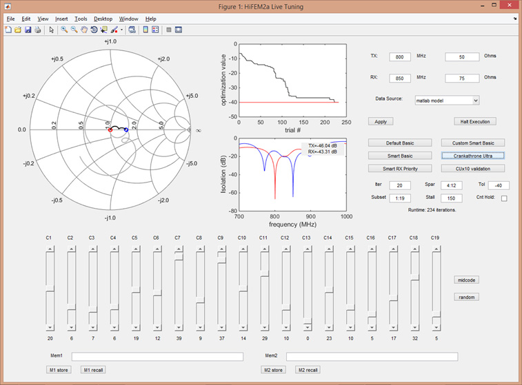
Up to this point in the story, I’ve left something out: the tuning problem. How do you find the magic settings that will give a dual-frequency solution among the roughly 1034 possible balance network configurations? (To describe this control problem as “astronomical” is understating it: there are only 1024 stars in the known universe.) During my architecture study, I had realized a way to dramatically simplify the control space by using the built-in filtering properties of the network to create semi-independent control knobs. While this brought it back into the realm of feasibility, the optimization problem was still a challenging one. I looked at various search and control algorithms known in literature such as genetic, particle swarm, and PCA, but in the end the thing that worked best was a custom algorithm which fully utilized the knowledge of the circuit architecture. I would have liked to try a neural network approach, which I think would have worked even better, but time did not allow. The Matlab GUI pictured here shows the automatic tuning interface which is able to tune and track the balance network in real-time.
Related Publications:
A Dual-Frequency 0.7-to-1GHz Balance Network for Electrical Balance Duplexers
B. Hershberg, B. van Liempd, X. Zhang, P. Wambacq, and J. Craninckx
In 2016 IEEE International Solid-State Circuits Conference (ISSCC), Jan, 2016.
» [Paper] [Slides] [DOI] [Abstract] [Bibtex]
@INPROCEEDINGS{2016-isscc-dual-frequency-balance-network,

author={B. Hershberg and B. van Liempd and X. Zhang and P. Wambacq and J. Craninckx},

booktitle={{2016 IEEE International Solid-State Circuits Conference (ISSCC)}},

title={{A Dual-Frequency 0.7-to-1GHz Balance Network for Electrical Balance Duplexers}},

year={2016},

pages={356-357},

abstract={An electrical-balance duplexer (EBD) is a tunable RF front-end concept that seeks to address several key challenges of 4G and 5G mobile systems [1]. The basic principle is shown in Fig. 20.8.1. Duplexer isolation is achieved when the signals in paths 1 and 2 cancel and prevent the TX signal from appearing at the RX port. This cancellation is achieved by “balancing” the antenna impedance ZANT with an on-chip tunable impedance ZBAL.},

keywords={Antennas;Bandwidth;CMOS integrated circuits;Filtering;Impedance;Mathematical model;Tuning},

doi={10.1109/ISSCC.2016.7418054},

month={Jan},

type={conference},}
2014 --- Gigasample High Linearity Ringamp Pipelined ADCs in 28nm
Gigasample High Linearity Ringamp Pipelined ADCs in 28nm
Technology: 16nm FinFET CMOS, 28nm CMOS
Time Period: 4 years (June 2014 – June 2018)
Collaborators: Jorge Lagos, Ewout Martens, Jan Craninckx
 When I decided to change continents and join imec in Belgium, it was always with the hope that I would be entering into an organization where I would have the chance to settle some unfinished PhD business. So, while I worked on RF related projects as my “day job”, I began pushing behind the scenes for a ringamp research program. The proposal was to venture into uncharted waters, towards higher speeds and order-of-magnitude breakthroughs in performance. This felt like an obvious next step to take in the topic, particularly at imec, where we had access to the latest and greatest nanoscale CMOS technologies.
A pilot project for this began in 2014 when we brought in a new PhD student, Jorge Lagos, to imec. We gave him the challenging goal of making a high linearity single-channel 1GS/s 10 ENOB pipelined ADC in 28nm CMOS. Perhaps this was a bit of a mean trick to play on an innocent and unsuspecting PhD student: planar 28nm CMOS is a something of a “worst case” technology for linearity. We figured if we could make it work in 28nm, we could make it work in anything. Fortunately, Jorge rose to the challenge and achieved impressive results, even hitting the 1GS/s target in his second chip. Jorge also invented some clever ideas for enhancing speed, linearity, and robustness. This resulted in several conference and journal papers. My involvement was to serve as a mentor and collaborator, both guiding the direction of research on a day-to-day basis and rolling up my sleeves to dig into the transistors when necessary.
The success of this research ultimately lead to getting a green light for the highly successful 16nm Ringamp ADC program that was launched in 2016. We learned many valuable lessons from the two chips in 28nm, and this carried through into subsequent 16nm designs not only in terms of what we chose to keep the same but also in terms of what we chose to do differently.
Related Publications:
A single-channel, 600Msps, 12bit, ringamp-based pipelined ADC in 28nm CMOS
J. Lagos, B. Hershberg, E. Martens, P. Wambacq, and J. Craninckx
In 2017 Symposium on VLSI Circuits, June, 2017.
» [Paper] [DOI] [Abstract] [Bibtex]
@INPROCEEDINGS{2017-vlsi-ringamp,

author={J. Lagos and B. Hershberg and E. Martens and P. Wambacq and J. Craninckx},

booktitle={{2017 Symposium on VLSI Circuits}},

title={{A single-channel, 600Msps, 12bit, ringamp-based pipelined ADC in 28nm CMOS}},

year={2017},

pages={C96-C97},

abstract={A pipelined ADC is presented that exploits the low but very constant (over output swing) open-loop gain characteristic of the ring amplifier (ringamp) to achieve high SFDR in low-voltage nanoscale CMOS designs. A dynamic ringamp biasing scheme using CMOS resistors and an active ringamp-based common-mode feedback (CMFB) are also introduced. The implemented prototype achieves 56.3dB SNDR and 69.2dB SFDR at 600Msps, consuming 14.2mW from a 0.9V supply, resulting in a Figure-of-Merit (FoM) of 44.3fJ/conv.-step.},

keywords={Architecture;Bandwidth;Linearity;Nanoscale devices;Resistors;Robustness;Steady-state},

doi={10.23919/VLSIC.2017.8008561},

month={June},

type={conference}}
A 1Gsps, 12-bit, single-channel pipelined ADC with dead-zone-degenerated ring amplifiers
J. Lagos, B. Hershberg, E. Martens, P. Wambacq, and J. Craninckx
In 2018 IEEE Custom Integrated Circuits Conference (CICC), April, 2018.
» [Paper] [DOI] [Abstract] [Bibtex]
@INPROCEEDINGS{2018-cicc-ringamp,

author={J. Lagos and B. Hershberg and E. Martens and P. Wambacq and J. Craninckx},

booktitle={{2018 IEEE Custom Integrated Circuits Conference (CICC)}},

title={{A 1Gsps, 12-bit, single-channel pipelined ADC with dead-zone-degenerated ring amplifiers}},

year={2018},

volume={},

number={},

pages={1-4},

abstract={The design of power-efficient ADCs able to achieve both high linearity and bandwidth in deep nanoscale CMOS processes becomes very challenging as the constraints of lowvoltage operation and limited intrinsic gain often mandate the use of power-consuming analog circuits and digital calibration. This work introduces a pipelined ADC that leverages the low but very flat open-loop gain vs. output swing characteristic of the ring amplifier (ringamp) to address these problems. A 12-bit, 1Gsps, single-channel prototype is implemented in a 28nm planar CMOS process achieving 56.6dB SNDR and 73.1dB SFDR. Consuming 24.8mW from a single 0.9V supply, it achieves Schreier and Walden FoMs of 159.6dB and 45fJ/conv.-step, respectively.},

keywords={Bandwidth;Calibration;Clocks;Frequency measurement;Linearity;Pipelines;Semiconductor device measurement;Pipelined ADC;dead-zone degeneration;gain calibration;ring amplifier;ringamp;single-channel},

doi={10.1109/CICC.2018.8357056},

ISSN={},

month={April},

type={conference}}
A Single-Channel, 600-MS/s, 12-b, Ringamp-Based Pipelined ADC in 28-nm CMOS
J. Lagos, B. Hershberg, E. Martens, P. Wambacq, and J. Craninckx
In IEEE Journal of Solid-State Circuits, Feb, 2019.
» [Paper] [DOI] [Abstract] [Bibtex]
@ARTICLE{2019-jssc-sp01-ringamp,

author={J. {Lagos} and B. {Hershberg} and E. {Martens} and P. {Wambacq} and J. {Craninckx}},

journal={{IEEE Journal of Solid-State Circuits}},

title={{A Single-Channel, 600-MS/s, 12-b, Ringamp-Based Pipelined ADC in 28-nm CMOS}},

year={2019},

volume={54},

number={2},

pages={403-416},

abstract={Achieving high linearity and bandwidth with good power efficiency makes the design of ADCs in deep nanoscale CMOS processes very challenging, as the constraints of low-voltage operation and limited intrinsic gain often dictate the use of power-consuming analog circuits and intensive digital calibration. This paper addresses these problems by introducing a pipelined ADC that exploits the low but very constant open-loop gain versus output voltage characteristic of the ring amplifier (ringamp) to achieve both high speed and linearity in low-voltage nanoscale CMOS designs. A tunable ringamp biasing scheme using an anti-parallel arrangement of CMOS transistors and an active ringamp-based common-mode feedback are also introduced. A single-channel prototype ADC is implemented in a standard 28-nm CMOS process, achieving 58.7-dB SNDR and 72.4-dB SFDR at 600 MS/s while consuming 14.5 mW from a single 0.9-V supply, resulting in Walden and Schreier figure-of-merit (FoM) values of 34.4 fJ/conv.-step and 161.9 dB, respectively.},

keywords={amplifiers;analogue-digital conversion;calibration;circuit feedback;CMOS digital integrated circuits;integrated circuit design;low-power electronics;nanoelectronics;power-consuming analog circuits;intensive digital calibration;pipelined ADC;ring amplifier;low-voltage nanoscale CMOS designs;anti-parallel arrangement;CMOS transistors;single-channel prototype ADC;low-voltage operation;limited intrinsic gain;constant open-loop gain;deep nanoscale CMOS process;active ring amp-based common-mode feedback;tunable ring amp biasing scheme;output voltage characteristic;single-channel ring amp-based pipelined ADC;ADC design;Schreier figure-of-merit;Walden figure-of-merit;power 14.5 mW;size 28 nm;voltage 0.9 V;V;Linearity;Resistance;Calibration;Transistors;Resistors;Inverters;Gain;Active common-mode feedback (CMFB);gain calibration;pipelined ADC;ring amplifier (ringamp);single channel},

doi={10.1109/JSSC.2018.2879923},

ISSN={0018-9200},

month={Feb},

type={journal}}
A 1-GS/s, 12-b, Single-Channel Pipelined ADC With Dead-Zone-Degenerated Ring Amplifiers
J. Lagos, B. Hershberg, E. Martens, P. Wambacq, and J. Craninckx
In IEEE Journal of Solid-State Circuits, March, 2019.
» [Paper] [DOI] [Abstract] [Bibtex]
@ARTICLE{2019-jssc-sp02-ringamp,

author={J. Lagos and B. Hershberg and E. Martens and P. Wambacq and J. Craninckx},

journal={{IEEE Journal of Solid-State Circuits}},

title={{A 1-GS/s, 12-b, Single-Channel Pipelined ADC With Dead-Zone-Degenerated Ring Amplifiers}},

year={2019},

volume={54},

number={3},

pages={646-658},

abstract={Ring amplification has recently been shown capable of simultaneously achieving high linearity and high bandwidth (BW) in low-voltage, deep nanoscale CMOS processes, while retaining good power efficiency. In these processes, the low but very flat open-loop (OL) gain versus output voltage characteristic of the ring amplifier can be exploited, together with its high BW, to overcome the low intrinsic gain limitations that otherwise mandate the use of power-consuming analog circuits and complex digital calibration. Within this context, this paper introduces the techniques of dead-zone degeneration (DZD) and second-stage bias enhancement to further extend the linearity and speed limits of the ring amplifier, respectively. These techniques are applied to a 12-b, 1-GS/s, single-channel pipelined ADC implemented in a 28-nm planar CMOS process, which achieves 56.6-dB SNDR and 73.1-dB SFDR while consuming 24.8 mW from a single 0.9-V supply, resulting in Schreier and Walden figure-of-merit (FoM) values of 159.6 dB and 45 fJ/conv.-step, respectively.},

keywords={Gain;Linearity;Voltage measurement;Calibration;Voltage control;Transconductance;Resistance;Bias enhancement;gain boosting;pipelined ADC;ring amplifier;ringamp;single-channel},

doi={10.1109/JSSC.2018.2889680},

ISSN={0018-9200},

month={March},

type={journal}}
2014 --- High Linearity Electrical Balance Duplexer for IBFD
High Linearity Electrical Balance Duplexer for IBFD
Technology: 180nm RF SOI CMOS
Time Period: 2 years (Sept 2013 – Aug 2015)
Collaborators: Barend van Liempd, Jan Craninckx
 Background: Modern mobile devices support several wireless standards and communicate on dozens of different frequency bands that span a vast swath of spectrum, particularly in the 800 MHz – 2.5 GHz range. Although fully-integrated software defined radios have evolved over the last decade to tackle this re-configurability challenge, the RF frontend “duplexer” sitting between the antenna and radio has not. As a result, most smartphones have many RF switches and fixed-frequency SAW filters placed around the radio IC on the circuit board, consuming significant physical area, performance, and cost.
One possible solution to this challenge is the idea of an Electrical Balance Duplexer (EBD). An EBD’s filtering/duplexing properties can be tuned by adjusting simple impedances, and it is possible to fully integrate it onto a single chip. The EBD works by passive signal cancellation, and this is particularly interesting because it makes it not only compatible with common FDD duplexing, but also with In-Band Full Duplex (IBFD) communication. IBFD is a potential 5G technology which allows a radio to transmit and receive on the same frequency at the same time.
HiFEM1 Project: My involvement in the EBD program at imec has spanned several projects, but centers around two core ones. The first project (codename HiFEM1), was to design a fully-integrated EBD that can meet the extremely stringent linearity specifications required for 3GPP FDD communication. To tackle this challenge, we moved into an RF SOI CMOS technology and used number of new architectural tricks to meet our targets. My role in the project was to design the balance network, which is the most critical block in terms of distortion. After a crash course in RF frontends, I researched techniques for building high-linearity RF switched capacitor arrays for the balance network. In measurement we achieved groundbreaking results which set the new state-of-the-art for linearity performance in EBDs, and published these findings at ISSCC 2015.
Related Publications:
A >70-dBm IIP3 Electrical-Balance Duplexer for Highly Integrated Tunable Front-Ends
B. van Liempd, B. Hershberg, S. Ariumi, K. Raczkowski, K. F. Bink, U. Karthaus, E. Martens, P. Wambacq, and J. Craninckx
In IEEE Transactions on Microwave Theory and Techniques, Dec, 2016.
» [Paper] [DOI] [Abstract] [Bibtex]
@ARTICLE{2016-tmtt-ebd,

author={B. van Liempd and B. Hershberg and S. Ariumi and K. Raczkowski and K. F. Bink and U. Karthaus and E. Martens and P. Wambacq and J. Craninckx},

journal={{IEEE Transactions on Microwave Theory and Techniques}},

title={{A >70-dBm IIP3 Electrical-Balance Duplexer for Highly Integrated Tunable Front-Ends}},

year={2016},

volume={64},

number={12},

pages={4274-4286},

abstract={An electrical-balance duplexer achieving the state-of-the-art linearity and insertion loss (IL) performance is presented, enabled by a partially depleted RF silicon-on-insulator CMOS technology. A single-ended configuration avoids the common-mode isolation problem suffered by topologies with a differential low-noise amplifier. Highly linear switched capacitors allow for impedance balancing to antennas with <;1.5:1 voltage standing wave ratio from 1.9 to 2.2 GHz. +70-dBm input-referred third-order intercept point is achieved under high transmitter (TX) power (+30.5 dBm max.). TX IL is <;3.7 dB, and receiver IL is <;3.9 dB.},
keywords={CMOS integrated circuits;differential amplifiers;low noise amplifiers;radiofrequency integrated circuits;silicon-on-insulator;IIP3 electrical-balance duplexer;RF silicon-on-insulator CMOS;antennas;differential low-noise amplifier;frequency 1.9 GHz to 2.2 GHz;highly integrated tunable front-ends;impedance balancing;insertion loss;linear switched capacitors;receiver;state-of-the-art linearity;transmitter;voltage standing wave ratio;Antennas;Distortion;Finite element analysis;Impedance;Jamming;Linearity;Radio frequency;CMOS integrated circuits;duplexer;electrical-balance (EB);frequency-division duplexing (FDD);hybrid transformer;linearity;silicon-on-insulator (SOI);tunable capacitors},
doi={10.1109/TMTT.2016.2613039},
ISSN={0018-9480},
month={Dec},
type={journal}}
An electrical-balance duplexer for in-band full-duplex with <-85dBm in-band distortion at +10dBm TX-power
B. van Liempd, B. Hershberg, B. Debaillie, P. Wambacq, and J. Craninckx
In European Solid-State Circuits Conference (ESSCIRC), ESSCIRC 2015 - 41st, Sept, 2015.
» [Paper] [DOI] [Abstract] [Bibtex]
@INPROCEEDINGS{2015-esscirc-ebd,

author={van Liempd, B. and Hershberg, B. and Debaillie, B. and Wambacq, P. and Craninckx, J.},

booktitle={{European Solid-State Circuits Conference (ESSCIRC), ESSCIRC 2015 - 41st}},

title={{An electrical-balance duplexer for in-band full-duplex with <-85dBm in-band distortion at +10dBm TX-power}},
year={2015},
pages={176-179},
abstract={When using electrical-balance duplexers (EBDs) to provide RF self-interference cancellation for in-band full-duplex, in-band distortion produced by nonlinear CMOS switches in the duplexer cause distortion that limits the headroom for additional self-interference cancellation in subsequent cancellation schemes in the transceiver. A prototype EBD is fabricated in 0.18μm SOI CMOS to investigate the dynamic range limitations of a transceiver architecture for next-generation wireless systems that supports in-band full-duplex and legacy FDD. Measurements show -85dBm in-band distortion at +10dBm TX input power, enough for short-range links at 10MHz BW.},
keywords={CMOS integrated circuits;frequency division multiplexing;interference suppression;multiplexing equipment;RF self-interference cancellation;SOI CMOS;bandwidth 10 MHz;dynamic range limitations;electrical-balance duplexers;in-band distortion;in-band full-duplex FDD;legacy FDD;next-generation wireless systems;nonlinear CMOS switches;prototype EBD;size 0.18 mum;transceiver architecture;Antenna measurements;Antennas;Distortion;Distortion measurement;Radio frequency;Silicon;Silicon carbide;In-band full-duplex;cancellation;electrical-balance duplexer;multi-tone test;self-interference},
doi={10.1109/ESSCIRC.2015.7313857},
ISSN={1930-8833},
month={Sept},
type={conference}}
A +70dBm IIP3 single-ended electrical-balance duplexer in 0.18um SOI CMOS
B. van Liempd, B. Hershberg, K. Raczkowski, S. Ariumi, U. Karthaus, K. Bink, and J. Craninckx
In Solid- State Circuits Conference - (ISSCC), 2015 IEEE International, Feb, 2015.
» [Paper] [DOI] [Abstract] [Bibtex]
@INPROCEEDINGS{2015-isscc-ebd,

author={van Liempd, Barend and Hershberg, Benjamin and Raczkowski, Kuba and Ariumi, Saneaki and Karthaus, Udo and Bink, Karl-Frederik and Craninckx, Jan},

booktitle={{Solid- State Circuits Conference - (ISSCC), 2015 IEEE International}},

title={{A +70dBm IIP3 single-ended electrical-balance duplexer in 0.18um SOI CMOS}},

year={2015},

month={Feb},

pages={1-3},

abstract={The electrical-balance (EB) duplexer concept explored in [1-4] suggests a possible integrated multiband alternative to conventional fixed-frequency surface-acoustic-wave (SAW) duplexers. The basic principle of the EB duplexer is to balance the impedances seen at the ports of a hybrid transformer to suppress signal transfer from the TX to the RX through signal cancellation (Fig. 2.2.1). While the potential payoff is tantalizing, several challenges must still be solved before EB duplexers can become commercially viable. Specifically, the duplexer must provide high isolation and linearity in both the TX and RX bands across wide bandwidth (BW), with low insertion loss (IL), all in the presence of a real antenna whose impedance is constantly varying due to real-world user interaction. In this paper, we present a duplexer that significantly advances the state-of-the-art for two of these critical challenges: linearity and insertion loss.},

keywords={Antenna measurements;Antennas;Capacitors;Impedance;Insertion loss;Linearity;Ports (Computers)},

doi={10.1109/ISSCC.2015.7062851},

type={conference},}
2013 --- VCO for Software Defined Radio
9-12 GHz VCO for Software Defined Radio
Technology: 28nm CMOS
Time Period: 9 months (Jan 2013 - Sept 2013)
Collaborators: Kuba Rackzkowsi, Jan Craninckx
 My first assignment at imec was to design a VCO operating from 9-12 GHz capable of supporting all major wireless standards including GSM, 3G, 4G, WiFi, and Bluetooth. This VCO was intended to provide the frequency reference for the frequency synthesizer in the 100 MHz - 6 GHz software defined radio program at imec known as "scaldio". In previous scaldio versions, there had been a number of problems with the VCO's, so my task was twofold: 1) make a robust and low power VCO, 2) explain what went wrong in past attempts. This project was my first foray into RF, and as such I learned quite a bit about RF in general during this time, and more specifically about the design of passives, quality-factor loss mechanisms, and VCO architectures.
During my investigations, I found that there were a number of design considerations that had been overlooked in the past, as well as some surprising behavior of the device models in the 28nm CMOS technology we were using which, in sum total, explained where the quality-factor losses had been coming from in the earlier designs. In the process of these investigations, I also invented a new circuit technique for biasing the floating nodes in the digitally controlled varactor array, which was later published at ESSCIRC 2014. There were a number of interesting things that I saw in the device models and EM simulations of the passives that I wanted to verify with actual silicon, so for the tapeout, four different VCOs were fabricated on a shared die. These four VCOs allowed for a differential comparison of certain design changes, which allowed us to draw our conclusions with confidence.
Final measured performance was remarkably well matched with expectation, which was of course a major relief for me since the main objective of this project was to make a well-understood design rather than break any power efficiency FoM records. Although it never saw its way into a full radio system due to the discontinuation of the scaldio program, it did make its way into a few PLLs and frequency synthesizers of other projects, and worked well for all of them. Phew!
Related Publications:
A DTC-Based Subsampling PLL Capable of Self-Calibrated Fractional Synthesis and Two-Point Modulation
N. Markulic, K. Raczkowski, E. Martens, P. P. E. Filho, B. Hershberg, P. Wambacq, and J. Craninckx
In IEEE Journal of Solid-State Circuits, Dec, 2016.
» [Paper] [DOI] [Abstract] [Bibtex]
@ARTICLE{2016-jssc-fnsspll-2pmod,

author={N. Markulic and K. Raczkowski and E. Martens and P. E. Paro Filho and B. Hershberg and P. Wambacq and J. Craninckx},

journal={{IEEE Journal of Solid-State Circuits}},

title={{A DTC-Based Subsampling PLL Capable of Self-Calibrated Fractional Synthesis and Two-Point Modulation}},

year={2016},

volume={51},

number={12},

pages={3078-3092},

abstract={We present an analog subsampling PLL based on a digital-to-time converter (DTC), which operates with almost no performance gap (176/198 fs RMS jitter) between the integer and the worst case fractional operation, achieving -246.6 dB FOM in the worst case fractional mode. The PLL is capable of two-point, 10 Mbit/s GMSK modulation with -40.5 dB EVM around a 10.24 GHz fractional carrier. The analog nonidealities-DTC gain, DTC nonlinearity, modulating VCO bank gain, and nonlinearity-are calibrated in the background while the system operates normally. This results in ~15 dB fractional spur improvement (from -41 dBc to -56.5 dBc) during synthesis and ~15 dB EVM improvement (from -25 dB to -40.5 dB) during modulation. The paper provides an overview of the mechanisms that contribute to performance degradation in DTC-based PLL/phase modulators and presents ways to mitigate them. We demonstrate state-of-the-art performance in nanoscale CMOS for fractional-N synthesis and phase modulation.},

keywords={digital-analogue conversion;minimum shift keying;phase locked loops;phase modulation;voltage-controlled oscillators;DTC gain;DTC nonlinearity;DTC-based analog subsampling PLL;VCO bank gain modulation;bit rate 10 Mbit/s;digital-to-time converter;nanoscale CMOS;phase modulators;self-calibrated fractional-N synthesis;two-point GMSK modulation;two-point modulation;Phase locked loops;Phase modulation;Quantization (signal);Voltage-controlled oscillators;Wideband;Analog PLL;GMSK;PLL;background calibration;digital-to-time converter (DTC);divider-less;fractional-N subsampling PLL (FNSSPLL);frequency synthesis;linearization;low jitter;phase/frequency modulation;polar modulation;subsampling PLL (SSPLL);two-point modulation;wideband modulation},

doi={10.1109/JSSC.2016.2596766},

ISSN={0018-9200},

month={Dec},

type={journal}}
A Self-Calibrated 10Mb/s Phase Modulator with -37.4dB EVM Based on a 10.1-to-12.4GHz, -246.6dB-FOM, Fractional-N Subsampling PLL
N. Markulic, K. Raczkowski, E. Martens, P. E. P. Filho, B. Hershberg, P. Wambacq, and J. Craninckx
In 2016 IEEE International Solid-State Circuits Conference (ISSCC), Jan, 2016.
» [Paper] [DOI] [Abstract] [Bibtex]
@INPROCEEDINGS{2016-isscc-fracn-sspll,

author={N. Markulic and K. Raczkowski and E. Martens and P. E. P. Filho and B. Hershberg and P. Wambacq and J. Craninckx},

booktitle={{2016 IEEE International Solid-State Circuits Conference (ISSCC)}},

title={{A Self-Calibrated 10Mb/s Phase Modulator with -37.4dB EVM Based on a 10.1-to-12.4GHz, -246.6dB-FOM, Fractional-N Subsampling PLL}},

year={2016},

pages={176-177},

abstract={The two-point injection scheme has proven to be an effective technique for overcoming the problem of PLL bandwidth limitations during wideband polar phase modulation [1]. The quality of the phase-modulated signal, typically expressed in terms of error-vector magnitude (EVM), still remains limited by the PLL phase-noise, gain mismatch between the two injection paths and linearity of the digital-to-modulated phase conversion. We present a phase modulator that makes use of an analog, fractional-N, digital-to-time-converter (DTC)-based subsampling PLL that achieves -37.4dB EVM around a 10.24GHz fractional carrier during 10Mb/s GMSK modulation. The subsampling PLL architecture uses no power-consuming divider and allows wide PLL bandwidth (because of its high phase-error detection gain) for optimal VCO noise suppression. The VCO has a secondary, digitally controlled capacitor bank (modulating DAC) used during two-point modulation. The gain errors and nonlinearities in the digital-to-modulated phase conversion are automatically background-calibrated in both injection points: in the phase-error detection path (where nonlinearity is dominated by the DTC INL) and in the VCO modulating capacitor bank (where nonlinearity is dominated by capacitor mismatch and nonlinear capacitance-to-frequency conversion).},

keywords={Calibration;Phase locked loops;Phase modulation;Solid state circuits;Table lookup;Voltage-controlled oscillators},

doi={10.1109/ISSCC.2016.7417964},

month={Jan},

type={conference},}
A 9.2-12.7 GHz Wideband Fractional-N Subsampling PLL in 28 nm CMOS With 280 fs RMS Jitter
K. Raczkowski, N. Markulic, B. Hershberg, and J. Craninckx
In Solid-State Circuits, IEEE Journal of, March, 2015.
» [Paper] [DOI] [Abstract] [Bibtex]
@ARTICLE{2015-jssc-subsampling-pll,

author={Raczkowski, K. and Markulic, N. and Hershberg, B. and Craninckx, J.},

journal={{Solid-State Circuits, IEEE Journal of}},

title={{A 9.2-12.7 GHz Wideband Fractional-N Subsampling PLL in 28 nm CMOS With 280 fs RMS Jitter}},

year={2015},

month={March},

volume={PP},

number={99},

pages={1-11},

abstract={This paper describes a fractional-N subsampling PLL in 28 nm CMOS. Fractional phase lock is made possible with almost no penalty in phase noise performance thanks to the use of a 10 bit, 0.55 ps/LSB digital-to-time converter (DTC) circuit operating on the sampling clock. The performance limitations of a practical DTC implementation are considered, and techniques for minimizing these limitations are presented. For example, background calibration guarantees appropriate DTC gain, reducing spurs. Operating at 10 GHz the system achieves −38 dBc of integrated phase noise (280 fs RMS jitter) when a worst case fractional spur of −43 dBc is present. In-band phase noise is at the level of −104 dBc/Hz. The class-B VCO can be tuned from 9.2 GHz to 12.7 GHz (32%). The total power consumption of the synthesizer, including the VCO, is 13 mW from 0.9 V and 1.8 V supplies.},

keywords={Delays;Phase locked loops;Phase modulation;Phase noise;Quantization (signal);Voltage-controlled oscillators;CMOS process;digital-controlled oscillators;digital-to-time converter;fractional-N;frequency synthesis;jitter;phase noise;phase-locked loops;radio transceivers;sampling;voltage-controlled oscillators},

doi={10.1109/JSSC.2015.2403373},

type={journal},

ISSN={0018-9200},}
A 9.2-12.7 GHz wideband fractional-N subsampling PLL in 28nm CMOS with 280fs RMS jitter
K. Raczkowski, N. Markulic, B. Hershberg, J. Van Driessche, and J. Craninckx
In Radio Frequency Integrated Circuits Symposium, 2014 IEEE, June, 2014.
» [Paper] [DOI] [Abstract] [Bibtex]
@INPROCEEDINGS{2014-rfic-subsampling-pll,

author={Raczkowski, K. and Markulic, N. and Hershberg, B. and Van Driessche, J. and Craninckx, J.},

booktitle={{Radio Frequency Integrated Circuits Symposium, 2014 IEEE}},

title={{A 9.2-12.7 GHz wideband fractional-N subsampling PLL in 28nm CMOS with 280fs RMS jitter}},

year={2014},

month={June},

pages={89-92},

abstract={This paper describes a fractional-N subsampling PLL in 28nm CMOS. Fractional lock is achieved by using a 10bit digital-to-time converter (DTC) that generates a delayed sampling clock with minimal impact on PLL performance. Background calibration guarantees appropriate DTC gain, reducing spurs. The system achieves -38 dBc of integrated phase noise (280fs RMS jitter) at 10GHz when a worst-case fractional spur of -43 dBc is present. In-band phase noise is at the level of -104 dBc/Hz. The class-B VCO used can be tuned from 9.2 GHz to 12.7 GHz (32%). The total power consumption of the synthesizer, including the VCO, is 13 mW from 0.9V and 1.8V supplies.},

keywords={CMOS integrated circuits;calibration;microwave integrated circuits;microwave oscillators;phase locked loops;voltage-controlled oscillators;CMOS;DTC;RMS jitter;background calibration;class-B VCO;digital-to-time converter;fractional lock;frequency 9.2 GHz to 12.7 GHz;in-band phase noise;power 13 mW;size 28 nm;time 280 fs;voltage 0.9 V;voltage 1.8 V;wideband fractional-N subsampling PLL;word length 10 bit;worst-case fractional spur;CMOS integrated circuits;Clocks;Delays;Jitter;Phase locked loops;Phase noise;Voltage-controlled oscillators;Phase locked loops;fractional-N;frequency synthesis;jitter;phase noise;sampling},

doi={10.1109/RFIC.2014.6851666},

ISSN={1529-2517},

type={conference},}
A 9.1-12.7 GHz VCO in 28nm CMOS with a bottom-pinning bias technique for digital varactor stress reduction
B. Hershberg, K. Raczkowski, K. Vaesen, and J. Craninckx
In European Solid State Circuits Conference (ESSCIRC), ESSCIRC 2014 - 40th, Sept, 2014.
» [Paper] [Slides] [DOI] [Abstract] [Bibtex]
@INPROCEEDINGS{2014-esscirc-bottom-pinning-vco,

author={Hershberg, B. and Raczkowski, K. and Vaesen, K. and Craninckx, J.},

booktitle={{European Solid State Circuits Conference (ESSCIRC), ESSCIRC 2014 - 40th}},

title={{A 9.1-12.7 GHz VCO in 28nm CMOS with a bottom-pinning bias technique for digital varactor stress reduction}},

year={2014},

month={Sept},

pages={83-86},

abstract={A wide tuning range class-B VCO in 28nm CMOS targeted for software defined radio applications demonstrates a technique for minimizing device stress while simultaneously optimizing off-state Q in digitally switched tank capacitor cells. The proposed digital varactor structure can be implemented using only capacitors and NMOS transistors, resulting in a very compact layout. The VCO operates between 9.1 - 12.7 GHz, achieving a tuning range of 32% and phase noise of -163.2 dBc/Hz at 20 MHz offset referred to a 915 MHz carrier while consuming 9.5 mW for a FoM of -187 dBc/Hz.},

keywords={CMOS analogue integrated circuits;MMIC oscillators;field effect MMIC;stress analysis;varactors;voltage-controlled oscillators;CMOS process;NMOS transistors;bottom-pinning bias technique;capacitors;device stress minimization;digital varactor stress reduction;digitally switched tank capacitor cells;frequency 9.1 GHz to 12.7 GHz;off-state Q optimization;phase noise;power 9.5 mW;size 28 nm;software defined radio;wide tuning range class-B VCO;CMOS integrated circuits;Stress;Transistors;Tuning;Varactors;Voltage-controlled oscillators},

doi={10.1109/ESSCIRC.2014.6942027},

ISSN={1930-8833},

type={conference},}
Projects at Oregon State University
Corvallis, Oregon, USA
2006 - 2012
2012 --- 15b Ringamp-only Pipelined ADC
15b Ringamp-only Pipelined ADC
Technology: 180nm CMOS
Time Period: approx. 6 months (2012)
Project Name: Hyperstack
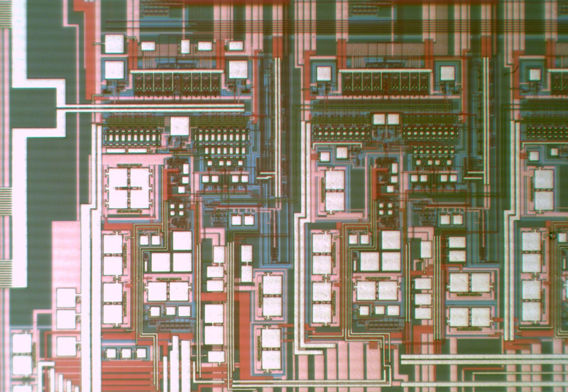 For my final project at OSU I wanted to target the same high accuracy specs of my previous 15b Ringamp Split-CLS pipelined ADC design, except this time I wanted to do it using ringamps only. This would establish that the ringamp is not only a good "assist" circuit, but also a standalone technique for reaching high accuracy in its own right.
I first tinkered around with fully differential ringamp designs, but had trouble ensuring common-mode stability due a number of factors specific to the technology and specific ringamp structure I was using. (A few years later Yong Lim at the University of Michigan figured out how to make it work). To work around this, I devised the idea of using a "composite ring amplifier block" which combines two pseudo-differential coarse ringamps with one differential input/single-ended output fine ringamp. This was a particularly interesting structure because it exploits a unique property of ringamps: self-cutoff. The coarse ringamps quickly charged into their dead-zone and automatically cut themselves off, leaving the fine ringamp with the correct differential and common mode levels needed for accurate differential settling despite only having a single ended output.
The implementation for this chip was a bit easier than earlier ones since I could reuse most of the 15b pipeline ADC of the previous project. The measured results showed a major improvement in power efficiency over the previous Split-CLS design, and achieved almost the same accuracy, this time with ringamps and nothing else. The results were presented at VLSI 2013 in Kyoto, Japan.
Related Publications:
Ring Amplification for Switched Capacitor Circuits
B. Hershberg
PhD Thesis, Oregon State University , June, 2012.
» [Paper] [Bibtex]
@phdthesis{2012-phdthesis-hershberg,

title={{Ring Amplification for Switched Capacitor Circuits}},

author={Hershberg, Benjamin},

school={Oregon State University},

year={2012},

month={June},

address={Corvallis, OR, USA},

type={thesis},

}
A 75.9dB-SNDR 2.96mW 29fJ/conv-step ringamp-only pipelined ADC
B. Hershberg and U. Moon
In VLSI Circuits (VLSIC), 2013 Symposium on, June, 2013.
» [Paper] [Abstract] [Bibtex]
@INPROCEEDINGS{2013-vlsi-composite-ringamp-block,

author={Hershberg, B. and Un-Ku Moon},

booktitle={{VLSI Circuits (VLSIC), 2013 Symposium on}},

title={{A 75.9dB-SNDR 2.96mW 29fJ/conv-step ringamp-only pipelined ADC}},

year={2013},

month={June},

pages={C94-C95},

abstract={A high resolution pipelined ADC that performs precision amplification using only ring amplifiers is presented. Several enabling techniques are introduced, namely parallelization via the use of Composite Ring Amplifier Blocks and a new ringamp topology designed for high-precision use. The 15b ADC achieves 75.9 dB SNDR and 91.4 dB SFDR at 1.2 V supply and 20 Msps conversion rate. Total power consumption is 2.96 mW, resulting in a Figure-of-Merit of 29 fJ/c-step.},

keywords={amplifiers;analogue-digital conversion;SFDR;SNDR;composite ring amplifier block;parallelization technique;pipelined ADC;power 2.96 mW;precision amplification;ringamp topology;voltage 1.2 V;Accuracy;Circuit stability;Inverters;Structural rings;Switched capacitor circuits;Switches;Very large scale integration},

type={conference},}
2011 --- 15b Split-CLS Ringamp ADC
15b Split-CLS Ringamp ADC
Technology: 180nm CMOS
Time Period: approx. 9 months (2011)
Project Name: Enceladus
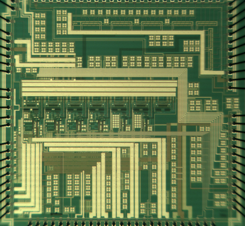 Before moving into ringamp-only research, I had some unfinished business to take care of. The initial motivation for the ringamp invention was my quest to find something to replace the ZCBC in the Split-CLS structure from my first chip. Whereas with a ZCBC I struggled to get above 11b ENOB, with the ringamp I could easily hit effective Split-CLS gains exceeding 110dB.
The limitations of working in a 180nm technology had a strong impact on my design decisions and the specs that I chose to target. On one hand, I knew that good intrinsic linearity of the transistors in 180nm would give me an advantage in pursuing high accuracy. On the other hand, I knew that I my speed and power efficiency would be heavily limited by the technology. Therefore, pursuing high accuracy ringamp circuits seemed the best thing to tackle first, with high speed and efficiency having to wait until I could get my hands on a newer technology.
In this chip I also put more effort into the architecture optimization. The 15b pipelined ADC used a 3b/stage MDAC and stage scaling. Due to the high accuracy targets, I also put effort into getting a good packaging and bonding setup, knowing that bondwire inductance could easily limit my performance if I wasn't careful.
The measured chip achieved very good performance, working more or less as expected (except for a crazy misunderstanding of the design rules which lead to me shorting my bootstrap switches to substrate!). It established the new state-of-the-art for power efficiency among all high accuracy ADCs. It was presented at ISSCC 2012 and later became an invited paper in the 2012 JSSC special edition. Chronologically, although I had designed my ringamp prototype chip first, this one was published first, making it the debut paper for the ring amplifier concept. Overall, I got a lot of enthusiastic feedback from people after my talk, and that excitement helped to set my trajectory and goals for many years to come.
Related Publications:
Ring amplifiers for switched-capacitor circuits
B. Hershberg, S. Weaver, K. Sobue, S. Takeuchi, K. Hamashita, and U. Moon
In Solid-State Circuits Conference Digest of Technical Papers (ISSCC), 2012 IEEE International, Feb, 2012.
» [Paper] [Slides] [DOI] [Abstract] [Bibtex]
@INPROCEEDINGS{2012-isscc-ringamp,

author={Hershberg, B. and Weaver, S. and Sobue, K. and Takeuchi, S. and Hamashita, K. and Un-Ku Moon},

booktitle={{Solid-State Circuits Conference Digest of Technical Papers (ISSCC), 2012 IEEE International}},

title={{Ring amplifiers for switched-capacitor circuits}},

year={2012},

month={Feb},

pages={460-462},

abstract={To overcome the challenges that CMOS process scaling has imposed on the design of switched-capacitor amplification circuits, designers must consider a growing number of design tradeoffs and employ new circuit techniques in order to achieve required accuracies, often at a cost of added power and complexity. This amplification performance bottleneck has been highlighted in recent years by the disparity in achievable power efficiency between SAR ADCs versus ADC structures that require amplification [1]. In many analog and mixed-signal topics, a comparison like this doesn't even exist, simply because amplification is a necessity. Even SAR ADCs have their limitations, particularly at higher resolutions where matching and noise constraints begin to dominate capacitor sizing and comparator power requirements.},

keywords={CMOS integrated circuits;amplifiers;analogue-digital conversion;integrated circuit design;switched capacitor networks;CMOS process scaling;SAR ADC structure;amplification performance;capacitor sizing;comparator power requirement;power efficiency;ring amplifier;switched-capacitor amplification circuit;Accuracy;Capacitors;Pipelines;Ring oscillators;Solid state circuits;Switches},

doi={10.1109/ISSCC.2012.6177090},

ISSN={0193-6530},

type={conference},}
The effect of correlated level shifting on noise performance in switched capacitor circuits
B. Hershberg, T. Musah, S. Weaver, and U. Moon
In Circuits and Systems (ISCAS), 2012 IEEE International Symposium on, May, 2012.
» [Paper] [Slides] [DOI] [Abstract] [Bibtex]
@INPROCEEDINGS{2012-iscas-cls-noise,

author={Hershberg, B. and Musah, T. and Weaver, S. and Un-Ku Moon},

booktitle={{Circuits and Systems (ISCAS), 2012 IEEE International Symposium on}},

title={{The effect of correlated level shifting on noise performance in switched capacitor circuits}},

year={2012},

month={May},

pages={942-945},

abstract={The relation between opamp noise and the size of the level shifting capacitor in correlated level-shifting (CLS) architectures is explored. Analysis is performed for a Split-CLS switched capacitor amplification circuit, and many of the conclusions in this paper are applicable to more general CLS architectures as well. A theoretical model for noise is developed and shown to be in good agreement with simulation. It is found that for practical design values, the size of the level-shifting capacitor only weakly influences noise performance.},

keywords={circuit noise;operational amplifiers;switched capacitor networks;correlated level shifting;general CLS architectures;level shifting capacitor;noise performance;opamp noise;split-CLS switched capacitor amplification circuit;switched capacitor circuits;Capacitance;Capacitors;Gain;Integrated circuit modeling;Noise;Transfer functions;Transistors},

doi={10.1109/ISCAS.2012.6272200},

ISSN={0271-4302},

type={conference},}
Ring Amplifiers for Switched Capacitor Circuits
B. Hershberg, S. Weaver, K. Sobue, S. Takeuchi, K. Hamashita, and U. Moon
In Solid-State Circuits, IEEE Journal of, Dec, 2012.
» [Paper] [DOI] [Abstract] [Bibtex]
@ARTICLE{2012-jssc-ringamp,

author={Hershberg, B. and Weaver, S. and Sobue, K. and Takeuchi, S. and Hamashita, K. and Un-Ku Moon},

journal={{Solid-State Circuits, IEEE Journal of}},

title={{Ring Amplifiers for Switched Capacitor Circuits}},

year={2012},

month={Dec},

volume={47},

number={12},

pages={2928-2942},

abstract={In this paper the fundamental concept of ring amplification is introduced and explored. Ring amplifiers enable efficient amplification in scaled environments, and possess the benefits of efficient slew-based charging, rapid stabilization, compression-immunity (inherent rail-to-rail output swing), and performance that scales with process technology. A basic operational theory is established, and the core benefits of this technique are identified. Measured results from two separate ring amplifier based pipelined ADCs are presented. The first prototype IC, a simple 10.5-bit, 61.5 dB SNDR pipelined ADC which uses only ring amplifiers, is used to demonstrate the core benefits. The second fabricated IC presented is a high-resolution pipelined ADC which employs the technique of Split-CLS to perform efficient, accurate amplification aided by ring amplifiers. The 15-bit ADC is implemented in a 0.18 μm CMOS technology and achieves 76.8 dB SNDR and 95.4 dB SFDR at 20 Msps while consuming 5.1 mW, achieving a FoM of 45 fJ/conversion-step.},

keywords={CMOS analogue integrated circuits;amplifiers;analogue-digital conversion;CMOS technology;SNDR pipelined ADC;Split-CLS;compression-immunity;power 5.1 mW;rapid stabilization;ring amplification;ring amplifier;size 0.18 micron;slew-based charging;switched capacitor circuit;word length 10.5 bit;word length 15 bit;Accuracy;CMOS integrated circuits;Gain;Inverters;Ring oscillators;Stability analysis;Transistors;A/D;ADC;CLS;RAMP;analog to digital conversion;analog to digital converter;correlated level shifting;high resolution;low power;nanoscale CMOS;rail-to-rail;ring amp;ring amplification;ring amplifier;ringamp;scalability;scaling;slew-based;split-CLS;stabilized ring oscillator;switched capacitor},

doi={10.1109/JSSC.2012.2217865},

ISSN={0018-9200},

type={journal},}
2011 --- Ringamp prototype ADC
Ringamp prototype ADC
Technology: 180nm CMOS
Time Period: approx. 9 months (2010/2011)
Project Name: Sagan
One of the toughest and most problematic blocks in my first chip at OSU was the zero-crossing based circuit. Despite its advantages it also came with a number of drawbacks. I felt that there must be a better way, and began to think about alternate ways to make a fast and efficient coarse-charging device. In the second half of 2009 I went to Atsugi, Japan for an internship at Asahei Kasei Microdevices (AKM). While riding trains around Japan on the weekends, I continued to ponder this, and by the time I had returned to OSU in 2010 I had a plan of attack. Within a few weeks, I figured out the blueprints for what I would later name the ring amplifier or "ringamp".
After developing the ringamp concept, I had two initial objectives in mind. The first was to make a basic prototype ADC by which to characterize the ringamp directly and get a good understanding of it's performance and behavior as well as to investigate any problems not predicted by simulation. This was also a direct request of my project promoters at AKM. Basically, ringamps seemed too good to be true and everyone wanted to see if they would even work in real silicon. They were particularly concerned about the noise performance.
The ringamp prototype ADC was a very basic 1.5b/stage pipeline architecture with no bells or whistles. It wasn't optimized for speed or power, only for learning about and characterizing the true performance of the ringamps inside. A huge hurdle in getting started was that I needed to do the design in AKM's native CAD tools. Fully setting that up on the OSU servers and integrating it with Calibre verification took me about 5 months of slow and halting efforts. Reading lots of PhD Comics during this time helped me to stay sane and laugh it off.
In measurement, I quickly saw encouraging results. Despite the lack of optimization and the 180nm technology, the performance was already quite competitive with state of the art and the core ringamp concept was successfully verified. I was ready to move on to more ambitious ringamp designs. This work was presented at VLSI 2012.
Related Publications:
Ring Amplifiers for Switched Capacitor Circuits
B. Hershberg, S. Weaver, K. Sobue, S. Takeuchi, K. Hamashita, and U. Moon
In Solid-State Circuits, IEEE Journal of, Dec, 2012.
» [Paper] [DOI] [Abstract] [Bibtex]
@ARTICLE{2012-jssc-ringamp,

author={Hershberg, B. and Weaver, S. and Sobue, K. and Takeuchi, S. and Hamashita, K. and Un-Ku Moon},

journal={{Solid-State Circuits, IEEE Journal of}},

title={{Ring Amplifiers for Switched Capacitor Circuits}},

year={2012},

month={Dec},

volume={47},

number={12},

pages={2928-2942},

abstract={In this paper the fundamental concept of ring amplification is introduced and explored. Ring amplifiers enable efficient amplification in scaled environments, and possess the benefits of efficient slew-based charging, rapid stabilization, compression-immunity (inherent rail-to-rail output swing), and performance that scales with process technology. A basic operational theory is established, and the core benefits of this technique are identified. Measured results from two separate ring amplifier based pipelined ADCs are presented. The first prototype IC, a simple 10.5-bit, 61.5 dB SNDR pipelined ADC which uses only ring amplifiers, is used to demonstrate the core benefits. The second fabricated IC presented is a high-resolution pipelined ADC which employs the technique of Split-CLS to perform efficient, accurate amplification aided by ring amplifiers. The 15-bit ADC is implemented in a 0.18 μm CMOS technology and achieves 76.8 dB SNDR and 95.4 dB SFDR at 20 Msps while consuming 5.1 mW, achieving a FoM of 45 fJ/conversion-step.},

keywords={CMOS analogue integrated circuits;amplifiers;analogue-digital conversion;CMOS technology;SNDR pipelined ADC;Split-CLS;compression-immunity;power 5.1 mW;rapid stabilization;ring amplification;ring amplifier;size 0.18 micron;slew-based charging;switched capacitor circuit;word length 10.5 bit;word length 15 bit;Accuracy;CMOS integrated circuits;Gain;Inverters;Ring oscillators;Stability analysis;Transistors;A/D;ADC;CLS;RAMP;analog to digital conversion;analog to digital converter;correlated level shifting;high resolution;low power;nanoscale CMOS;rail-to-rail;ring amp;ring amplification;ring amplifier;ringamp;scalability;scaling;slew-based;split-CLS;stabilized ring oscillator;switched capacitor},

doi={10.1109/JSSC.2012.2217865},

ISSN={0018-9200},

type={journal},}
A 61.5dB SNDR pipelined ADC using simple highly-scalable ring amplifiers
B. Hershberg, S. Weaver, K. Sobue, S. Takeuchi, K. Hamashita, and U. Moon
In VLSI Circuits (VLSIC), 2012 Symposium on, June, 2012.
» [Paper] [Slides] [DOI] [Abstract] [Bibtex]
@INPROCEEDINGS{2012-vlsi-ringamp,

author={Hershberg, B. and Weaver, S. and Sobue, K. and Takeuchi, S. and Hamashita, K. and Un-Ku Moon},

booktitle={{VLSI Circuits (VLSIC), 2012 Symposium on}},

title={{A 61.5dB SNDR pipelined ADC using simple highly-scalable ring amplifiers}},

year={2012},

month={June},

pages={32-33},

abstract={A ring amplifier based pipelined ADC is presented that uses simple cells constructed from small inverters and capacitors to perform amplification. The basic ring amplifier structure is characterized and demonstrated to be highly scalable, power efficient, and compression-immune (inherent rail-to-rail output swing). The prototype 10.5-bit ADC, fabricated in 0.18μm CMOS technology, achieves 61.5dB SNDR at a 30MHz sampling rate and consumes 2.6mW, resulting in a FoM of 90fJ/conversion-step.},

keywords={CMOS integrated circuits;amplifiers;analogue-digital conversion;10.5-bit ADC;CMOS technology;SNDR pipelined ADC;capacitor;compression-immune;frequency 30 MHz;inherent rail-to-rail output swing;noise figure 61.5 dB;power efficient;ring amplifier based pipelined ADC;ring amplifier structure;Accuracy;CMOS integrated circuits;CMOS technology;Digital audio players;Inverters;Structural rings;Transistors},

doi={10.1109/VLSIC.2012.6243775},

type={conference},}
2009 --- Pipelined ADC with Split-CLS technique and Zero Crossing Based Circuit
Pipelined ADC with Split-CLS technique and Zero Crossing Based Circuit
Technology: 180nm BiCMOS
Time Period: approx. 1.5 year (2008/2009)
Project Name: Locutus
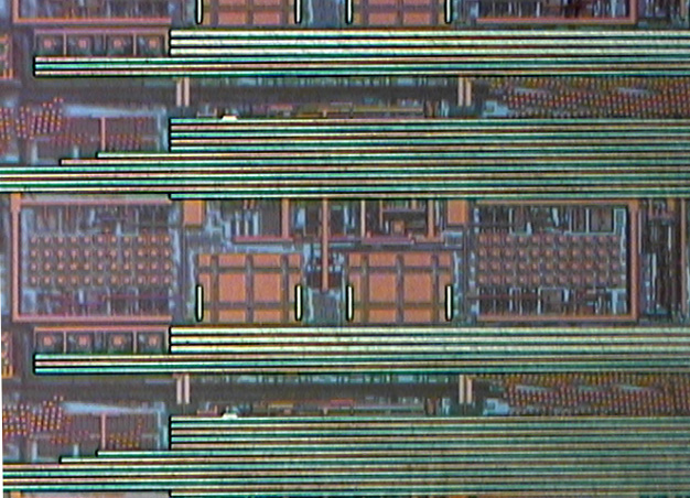 My first chip! When I started my PhD in 2006 under Dr. Un-Ku Moon, I'd never taken a class in any analog mixed-signal or RF topics and had no exposure to IC design. In undergrad I was more interested in CS related topics. So it took a few years to get up to speed before I could do any useful research. But by late 2007 I was beginning to generate ideas, and a few of them weren't entirely terrible. One of the techniques that my office mate Rob Gregoire had recently invented was Correlated Level Shifting (CLS), which is a compelling approach to suppressing the finite gain error of opamps in switched capacitor feedback circuits. Another idea that made a strong impression on me early on was zero-crossing based circuits (ZCBC), an idea which came out of Dr. Harry Lee's group at MIT and debuted during my first time at ISSCC in 2006.
My first chip was born out of explorations into those two ideas. I eventually saw that CLS could be implemented in a more generic form that relaxed the amplifier requirements, and I nicknamed this Split-CLS. Furthermore, I realized that Split-CLS could be used to linearize a ZCBC, or alternately that a ZCBC could be used as a coarse charging device alongside an opamp in Split-CLS. For this chip, I combined a ZCBC and a telescopic opamp using Split-CLS to form a high accuracy, high efficiency switched capacitor amplification circuit. One of the most direct ways to characterize such an amplifier idea is by using it in the MDAC of a Pipelined ADC. And so off I went.
When I finally got the chip in the lab and started getting good data out of it, I was pretty blown away. You see the simulation results, but it's hard to believe that an IC is actually doing all of it's electron manipulation magic until you have it in the lab and see the real data. Like any first attempt, I knew in retrospect that there were many things I'd do differently the second time around. But still, I had a working chip with good enough results to submit to ISSCC, so I was pretty stoked. I got extremely lucky and my paper was accepted - the numbers weren't amazing but people liked the idea. This was hugely exciting for me at the time, and served as a great motivator and confidence booster.
Related Publications:
The effect of correlated level shifting on noise performance in switched capacitor circuits
B. Hershberg, T. Musah, S. Weaver, and U. Moon
In Circuits and Systems (ISCAS), 2012 IEEE International Symposium on, May, 2012.
» [Paper] [Slides] [DOI] [Abstract] [Bibtex]
@INPROCEEDINGS{2012-iscas-cls-noise,

author={Hershberg, B. and Musah, T. and Weaver, S. and Un-Ku Moon},

booktitle={{Circuits and Systems (ISCAS), 2012 IEEE International Symposium on}},

title={{The effect of correlated level shifting on noise performance in switched capacitor circuits}},

year={2012},

month={May},

pages={942-945},

abstract={The relation between opamp noise and the size of the level shifting capacitor in correlated level-shifting (CLS) architectures is explored. Analysis is performed for a Split-CLS switched capacitor amplification circuit, and many of the conclusions in this paper are applicable to more general CLS architectures as well. A theoretical model for noise is developed and shown to be in good agreement with simulation. It is found that for practical design values, the size of the level-shifting capacitor only weakly influences noise performance.},

keywords={circuit noise;operational amplifiers;switched capacitor networks;correlated level shifting;general CLS architectures;level shifting capacitor;noise performance;opamp noise;split-CLS switched capacitor amplification circuit;switched capacitor circuits;Capacitance;Capacitors;Gain;Integrated circuit modeling;Noise;Transfer functions;Transistors},

doi={10.1109/ISCAS.2012.6272200},

ISSN={0271-4302},

type={conference},}
A 1.4V signal swing hybrid CLS-opamp/ZCBC pipelined ADC using a 300mV output swing opamp
B. Hershberg, S. T. Weaver, and U. Moon
In Solid-State Circuits Conference Digest of Technical Papers (ISSCC), 2010 IEEE International, Feb, 2010.
» [Paper] [Slides] [DOI] [Abstract] [Bibtex]
@INPROCEEDINGS{2010-isscc-split-cls-zcbc,

author={Hershberg, B. and Weaver, S.T. and Un-Ku Moon},

booktitle={{Solid-State Circuits Conference Digest of Technical Papers (ISSCC), 2010 IEEE International}},

title={{A 1.4V signal swing hybrid CLS-opamp/ZCBC pipelined ADC using a 300mV output swing opamp}},

year={2010},

month={Feb},

pages={302-303},

abstract={A Hybrid CLS-opamp/ZCBC pipelined ADC is introduced to improve accuracy, robustness, and power efficiency. Fast and accurate residue amplification is achieved by invoking a short ZCBC operation followed by CLS-opamp settling. Measured ENOB is better than 11 b at sampling rate of 20 MHz.},

keywords={CMOS integrated circuits;analogue-digital conversion;operational amplifiers;pipeline arithmetic;ENOB;correlated level-shifting;frequency 20 MHz;residue amplification;signal swing hybrid CLS-Opamp-ZCBC pipelined ADC;voltage 1.4 V;voltage 300 mV;voltage output swing opamp;zero-crossing based circuits;CMOS technology;Pipelines;Robustness;Sampling methods;Switches;Tail;Temperature;Testing;Timing;Voltage},

doi={10.1109/ISSCC.2010.5433894},

ISSN={0193-6530},

type={conference},}
Asynchronous CLS for Zero Crossing based Circuits
H. Venkatram, B. Hershberg, and U. Moon
In Electronics, Circuits, and Systems (ICECS), 2010 17th IEEE International Conference on, Dec, 2010.
» [Paper] [DOI] [Abstract] [Bibtex]
@INPROCEEDINGS{2010-icecs-asynchronous-cls,

author={Venkatram, H. and Hershberg, B. and Un-Ku Moon},

booktitle={{Electronics, Circuits, and Systems (ICECS), 2010 17th IEEE International Conference on}},

title={{Asynchronous CLS for Zero Crossing based Circuits}},

year={2010},

month={Dec},

pages={1025-1028},

abstract={This paper introduces Asynchronous correlated level shifting (ACLS) for Zero Crossing based Circuits. ACLS technique for Zero crossing based circuits provides rail-to-rail, asynchronous operation for the estimation and level shifting phase. The current source non-linearity is reduced and the power supply rejection ratio is improved.},

keywords={operational amplifiers;ACLS technique;asynchronous CLS;asynchronous correlated level shifting;current source nonlinearity;level shifting phase;power supply rejection ratio;rail-to-rail asynchronous operation;zero crossing-based circuits;Capacitors;ACLS;Rail-to-Rail operation;ZCBC},

doi={10.1109/ICECS.2010.5724689},

type={conference},}
Design of a Split-CLS Pipelined ADC With Full Signal Swing Using an Accurate But Fractional Signal Swing Opamp
B. Hershberg, S. Weaver, and U. Moon
In Solid-State Circuits, IEEE Journal of, Dec, 2010.
» [Paper] [DOI] [Abstract] [Bibtex]
@ARTICLE{2010-jssc-split-cls-adc,

author={Hershberg, B. and Weaver, S. and Un-Ku Moon},

journal={{Solid-State Circuits, IEEE Journal of}},

title={{Design of a Split-CLS Pipelined ADC With Full Signal Swing Using an Accurate But Fractional Signal Swing Opamp}},

year={2010},

month={Dec},

volume={45},

number={12},

pages={2623-2633},

abstract={Building on the technique of correlated level shifting (CLS), Split-CLS is introduced as a viable way to enable the design of high performance, high resolution A/D converters in deep submicron CMOS processes. One possible implementation of Split-CLS is presented, which achieves very high effective gain, and combines the fast, high efficiency charging of a zero-crossing based circuit (ZCBC) with the high-accuracy, low power settling of a double-cascode telescopic opamp. A dynamic zero-crossing detector (ZCD) conserves power in the ZCBC by only creating high bandwidth in the ZCD near the zero-crossing instant. Measured results are presented from a pipelined A/D converter fabricated in 0.18 m CMOS. Using the Split-CLS structure, an opamp with 300 mV output swing is used to produce a pipeline stage output swing of 1.4 V. The proof-of-concept test chip achieves 68.3 dB SNDR (11.1b ENOB) and 76.3dB SFDR while sampling at 20 MHz, and consumes 17.2 mW at 1.8 V supply.},

keywords={CMOS integrated circuits;analogue-digital conversion;network synthesis;operational amplifiers;A/D converters;CMOS process;correlated level shifting;design;full signal swing;signal swing opamp;split-CLS pipelined ADC;zero-crossing based circuit;zero-crossing detector;Analog-digital conversion;Calibration;Capacitors;Switching circuits;Transistors;A/D;ADC;CBSC;CLS;Split-CLS;ZCBC;ZCD;comparator based switched capacitor circuit;correlated level shifting;dynamic zero crossing detector;pipelined analog-to-digital converter;scaled CMOS amplification technique;switched capacitor amplification;zero crossing based circuit},

doi={10.1109/JSSC.2010.2073190},

ISSN={0018-9200},

type={journal},}